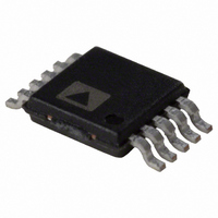
AD5624RBRMZ-5 Analog Devices Inc, AD5624RBRMZ-5 Datasheet - Page 22

AD5624RBRMZ-5
Manufacturer Part Number
AD5624RBRMZ-5
Description
IC DAC NANO 12BIT 2.5V 10-MSOP
Manufacturer
Analog Devices Inc
Series
nanoDAC™r
Specifications of AD5624RBRMZ-5
Data Interface
DSP, MICROWIRE™, QSPI™, Serial, SPI™
Settling Time
3µs
Number Of Bits
12
Number Of Converters
4
Voltage Supply Source
Single Supply
Operating Temperature
-40°C ~ 105°C
Mounting Type
Surface Mount
Package / Case
10-MSOP, Micro10™, 10-uMAX, 10-uSOP
Resolution (bits)
12bit
Sampling Rate
287kSPS
Input Channel Type
Serial
Supply Voltage Range - Analog
2.7V To 3.6V, 4.5V To 5.5V
Supply Current
950µA
Number Of Channels
4
Resolution
12b
Conversion Rate
287KSPS
Interface Type
Serial (3-Wire, SPI, QSPI, Microwire)
Single Supply Voltage (typ)
5V
Dual Supply Voltage (typ)
Not RequiredV
Architecture
Resistor-String
Power Supply Requirement
Single
Output Type
Voltage
Integral Nonlinearity Error
±1LSB
Single Supply Voltage (min)
4.5V
Single Supply Voltage (max)
5.5V
Dual Supply Voltage (min)
Not RequiredV
Dual Supply Voltage (max)
Not RequiredV
Operating Temp Range
-40C to 105C
Operating Temperature Classification
Industrial
Mounting
Surface Mount
Pin Count
10
Package Type
MSOP
Lead Free Status / RoHS Status
Lead free / RoHS Compliant
Power Dissipation (max)
-
Lead Free Status / Rohs Status
Compliant
Available stocks
Company
Part Number
Manufacturer
Quantity
Price
Part Number:
AD5624RBRMZ-5
Manufacturer:
ADI/亚德诺
Quantity:
20 000
AD5624R/AD5644R/AD5664R
POWER-ON RESET
The AD5624R/AD5644R/AD5664R family contains a power-on
reset circuit that controls the output voltage during power-up.
The output of the AD5624R/AD5644R/AD5664R DACs powers
up to 0 V and the output remains there until a valid write
sequence is made to the DACs. This is useful in applications
where it is important to know the state of the output of the
DACs while they are in the process of powering up.
SOFTWARE RESET
The AD5624R/AD5644R/AD5664R contain a software reset
function. Command 101 is reserved for the software reset
function (see Table 8). The software reset command contains
two reset modes that are software programmable by setting bit
DB0 in the control register.
Table 10 shows how the state of the bit corresponds to the
software reset modes of operation of the devices.
Table 12 shows the contents of the input shift register during the
software reset mode of operation.
Table 10. Software Reset Modes for the
AD5624R/AD5644R/AD5664R
DB0
0
1 (Power-On Reset)
POWER-DOWN MODES
The AD5624R/AD5644R/AD5664R contain four separate modes
of operation. Command 100 is reserved for the power-down
function (see Table 8). These modes are software programmable
by setting two bits (DB5 and DB4) in the control register. Table 11
shows how the state of the bits corresponds to the mode of
operation of the device. All DACs (DAC D to DAC A) can be
powered down to the selected mode by setting the correspond-
ing four bits (DB3, DB2, DB1, and DB0) to 1.
Table 12. 24-Bit Input Shift Register Contents for Software Reset Command
DB23 to DB22 (MSB)
x
Don’t care
Table 13. 24-Bit Input Shift Register Contents of Power-Down/Power-Up Operation for the AD5624R/AD5644R/AD5664R
DB23 to
DB22
(MSB)
x
Don’t
care
DB21
1
Command bits (C2 to C0)
DB20
0
Registers Reset to 0
DAC register
Input shift register
DAC register
Input shift register
LDAC register
Power-down register
Internal reference setup register
DB21
1
Command bits (C2 to C0)
DB19
0
DB20
0
DB18
x
Address bits (A2 to A0)
DB19
1
Don’t care
DB17
x
DB18
x
Address bits (A2 to A0)
Rev. B | Page 22 of 28
DB16
x
DB17
x
DB15
to DB6
x
Don’t
care
By executing the same Command 100, any combination of DACs
can be powered up by setting the bits (DB5 and DB4) to normal
operation mode. To select which combination of DAC channels
to power-up, set the corresponding four bits (DB3, DB2, DB1,
and DB0) to 1. See Table 13 for contents of the input shift register
during power-down/power-up operation.
Table 11.
AD5664R
DB5
0
0
1
1
When Bit DB5 and Bit DB4 are set to 0, the part works normally
with its normal power consumption of 450 μA at 5 V. However,
for the three power-down modes, the supply current falls to
480 nA at 5 V (200 nA at 3 V). Not only does the supply current
fall, but the output stage is also internally switched from the
output of the amplifier to a resistor network of known values.
This allows the output impedance of the part to be known while
the part is in power-down mode. The outputs can either be
connected internally to GND through a 1 kΩ resistor, or left
open-circuited (three-state) as shown in Figure 56.
The bias generator, the output amplifier, the resistor string, and
other associated linear circuitry are shutdown when power-down
mode is activated. However, the contents of the DAC register are
unaffected when in power-down. The time to exit power-down
is typically 4 μs for V
DB16
x
STRING DAC
RESISTOR
0
DB4
1
0
1
DB5
PD1
Modes of Operation for the AD5624R/AD5644R/
DB15 to DB1
x
Don’t care
Power-down
Figure 56. Output Stage During Power-Down
mode
Operating Mode
Normal operation
Power-down mode: 1 kΩ to GND
Power-down mode: 100 kΩ to GND
Power-down mode: three-state
DB4
PD0
DD
POWER-DOWN
= 5 V and for V
AMPLIFIER
CIRCUITRY
DB3
DAC D
selection, set bit to 1 to select channel
DB0 (LSB)
1/0
Determines software reset mode
Power-down/power-up channel
DB2
DAC C
DD
RESISTOR
NETWORK
= 3 V (see Figure 39).
DB1
DAC B
V
OUT
DB0
(LSB)
DAC A


