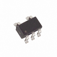
MAX5362MEUK+T Maxim Integrated Products, MAX5362MEUK+T Datasheet - Page 10

MAX5362MEUK+T
Manufacturer Part Number
MAX5362MEUK+T
Description
IC DAC 6BIT LP 2WIRE SER SOT23-5
Manufacturer
Maxim Integrated Products
Datasheet
1.MAX5362LEUKT.pdf
(13 pages)
Specifications of MAX5362MEUK+T
Settling Time
20µs
Number Of Bits
6
Data Interface
Serial
Number Of Converters
1
Voltage Supply Source
Single Supply
Operating Temperature
-40°C ~ 85°C
Mounting Type
Surface Mount
Package / Case
SOT-23-5, SC-74A, SOT-25
Number Of Dac Outputs
1
Resolution
6 bit
Interface Type
Serial (I2C)
Supply Voltage (max)
5.5 V
Supply Voltage (min)
2.7 V
Maximum Operating Temperature
+ 85 C
Mounting Style
SMD/SMT
Minimum Operating Temperature
- 40 C
Supply Current
230 uA
Voltage Reference
Internal
Lead Free Status / RoHS Status
Lead free / RoHS Compliant
Power Dissipation (max)
-
Lead Free Status / Rohs Status
Lead free / RoHS Compliant
Other names
MAX5362MEUK+T
condition (Figure 6). The bus is then free for another
transmission.
SDA’s state is sampled, and therefore must remain sta-
ble while SCL is high. Data is transmitted in 8-bit bytes.
Nine clock cycles are required to transfer each byte to
the MAX5360/MAX5361/MAX5362. Release SDA during
the 9th clock cycle as the selected device acknowl-
edges the receipt of the byte, by pulling SDA low dur-
ing this time. A series resistor on the SDA line may be
needed if the master’s output is forced high while the
selected device acknowledges (Figure 4).
The MAX5360/MAX5361/MAX5362 are available with
one of four preset slave addresses. Each address
Low-Cost, Low-Power 6-Bit DACs with
2-Wire Serial Interface in SOT23 Package
Figure 5. Start and Stop Conditions
Figure 6. Complete Serial Transmission
10
SDA
SCL
SDA
SCL
CONDITION
______________________________________________________________________________________
START
START CONDITION
MSB
0
1
1
2
1
3
SLAVE ADDRESS BYTE
0
4
0
5
Slave Address
X
6
STOP CONDITION
LSB
X
7
SHDN
8
ACK
9
option is identified by the suffix L, M, N, or P added to
the part number. The address is defined as the 7 most
significant bits (MSBs) sent by the master after a
START condition. The address options are 0x60, 0x62,
0x64, and 0x66 (left justified with LSB set to 0). The 8th
bit, typically used to define a write or read protocol,
sets the device’s power mode (SHDN); the device is
powered down when SHDN is set to 1. During a device
search routine, the MAX5360/MAX5361/MAX5362
acknowledge both options (SHDN = 0 or SHDN = 1)
but does not change its power state if a stop condition
(or restart) is issued immediately. The second byte
(DAC data) must be sent/received for the device to
update both power mode and DAC output.
The 6-bit DAC data is decoded as straight binary MSB
first with 1LSB = (V
responding analog voltage as shown in Table 1. Two
subbits complete the data byte; these 2 bits should be
set to zero since they are not tested to guaranteed-
monotonic performance.
After receiving the data byte, the MAX5360/MAX5361/
MAX5362 acknowledge its receipt and expect a STOP
condition, at which point the DAC output is updated.
The devices update the output and the power mode
only if the second byte is clocked in (SHDN = 0) or out
(SHDN = 1) of the device. When SHDN = 1, the master
will read all ones when clocking out a data byte. The
MAX5360/MAX5361/MAX5362 do not drive SDA except
for the acknowledge bit.
MSB
D6
10
D4
11
D3
12
D2
13
DAC CODE
REF
/ 64) and converted into the cor-
D1
14
D0
15
S1
16
LSB
S0
17
DAC Data
18
ACK
CONDITION
STOP


