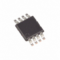
MAX5512EUA+ Maxim Integrated Products, MAX5512EUA+ Datasheet - Page 19

MAX5512EUA+
Manufacturer Part Number
MAX5512EUA+
Description
IC DAC 8BIT DUAL VOUT 8-UMAX
Manufacturer
Maxim Integrated Products
Datasheet
1.MAX5512EUA.pdf
(23 pages)
Specifications of MAX5512EUA+
Settling Time
660µs
Number Of Bits
8
Data Interface
Serial
Number Of Converters
2
Voltage Supply Source
Single Supply
Operating Temperature
-40°C ~ 85°C
Mounting Type
Surface Mount
Package / Case
8-MSOP, Micro8™, 8-uMAX, 8-uSOP,
Number Of Dac Outputs
2
Resolution
8 bit
Interface Type
Serial (SPI)
Supply Voltage (max)
5.5 V
Supply Voltage (min)
1.8 V
Maximum Operating Temperature
+ 85 C
Mounting Style
SMD/SMT
Minimum Operating Temperature
- 40 C
Supply Current
0.006 mA
Voltage Reference
External
Lead Free Status / RoHS Status
Lead free / RoHS Compliant
Power Dissipation (max)
-
Lead Free Status / Rohs Status
Lead free / RoHS Compliant
Figure
Greater-than-Unity DAC Gains Using the Same Reference
See the circuit in
use the MAX5515 to bias a two-electrode potentiostat
on the input of an ADC.
Bypass the power supply with a 0.1µF capacitor to GND.
Minimize lengths to reduce lead inductance. If noise
becomes an issue, use shielding and/or ferrite beads to
increase isolation. For the thin QFN package, connect the
exposed pad to ground.
Digital and AC transient signals coupling to GND can
create noise at the output. Use proper grounding tech-
niques, such as a multilayer board with a low-inductance
ground plane. Wire-wrapped boards and sockets are not
recommended. For optimum system performance, use
printed circuit (PC) boards. Good PC board ground lay-
out minimizes crosstalk between DAC outputs, reference
inputs, and digital inputs. Reduce crosstalk by keeping
analog lines away from digital lines.
REFIN
8. Separate Force-Sense Outputs Create Unity and
DAC
DAC
1/2 MAX5514
Figure
______________________________________________________________________________________
Layout Considerations
Self-Biased Two-Electrode
Bypassing Considerations
Potentiostat Application
10 for an illustration of how to
FBA
FBB
VOUTA
VOUTB
Power Supply and
R2
R1
N
OF THE DAC A INPUT CODE.
N
OF THE DAC B INPUT CODE.
V
V
V
V
DACA
DACB
OUT1
OUT1
OUT2
OUT2
=
IS THE NUMERIC VALUE
=
IS THE NUMERIC VALUE
V
V
REFIN
REFIN
256
256
× N
× N
DACA
DACB
(
1 +
8-Bit, Voltage-Output DACs
R2
R1
)
Dual, Ultra-Low-Power,
Figure
Figure
SCLK
CS1
CS2
DIN
9. Software-Configurable Output Gain
10. Self-Biased Two-Electrode Potentiostat Application
REFIN
REF
DAC
BAND
GAP
1/2 MAX5514
1/2 MAX5515
DAC
1.8V ≤ V
N
N
DD
DAC
POT
≤ 5.5V
FB
IS THE NUMERIC VALUE OF THE POT INPUT CODE.
IS THE NUMERIC VALUE OF THE DAC INPUT CODE.
REFOUT
V
OUT
OUT
FB
=
V
REFIN
I
256
F
W
SENSOR
× N
VOUT
WE
CE
DAC
R
(
C
F
1 +
H
L
L
255 - N
RATIOMETRIC
MAX5401
SOT-POT
5PPM/°C
255
100kΩ
TEMPCO
TO ADC
TO ADC
TO ADC
POT
)
V
OUT
19


