DAC0808LCN/NOPB National Semiconductor, DAC0808LCN/NOPB Datasheet - Page 4
DAC0808LCN/NOPB
Manufacturer Part Number
DAC0808LCN/NOPB
Description
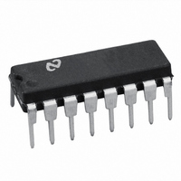
IC CONVERTER D/A 8BIT 16-DIP
Manufacturer
National Semiconductor
Datasheet
1.DAC0808LCMNOPB.pdf
(12 pages)
Specifications of DAC0808LCN/NOPB
Settling Time
150ns
Number Of Bits
8
Data Interface
Parallel
Number Of Converters
1
Voltage Supply Source
Single Supply
Power Dissipation (max)
305mW
Operating Temperature
0°C ~ 75°C
Mounting Type
Through Hole
Package / Case
16-DIP (0.300", 7.62mm)
Lead Free Status / RoHS Status
Lead free / RoHS Compliant
Other names
*DAC0808LCN
*DAC0808LCN/NOPB
DAC0808
DAC0808LCN
*DAC0808LCN/NOPB
DAC0808
DAC0808LCN
Available stocks
Company
Part Number
Manufacturer
Quantity
Price
Company:

Part Number:
DAC0808LCN/NOPB
Manufacturer:
NEC
Quantity:
2 300


www.national.com
(V
Electrical Characteristics
Note 2: Absolute Maximum Ratings indicate limits beyond which damage to the device may occur. DC and AC electrical specifications do not apply when operating
the device beyond its specified operating conditions.
Note 3: Range control is not required.
Note 4: The maximum power dissipation must be derated at elevated temperatures and is dictated by T
allowable power dissipation at any temperature is P
T
package, this number increases to 175˚C/W and for the small outline M package this number is 100˚C/W.
Note 5: Human body model, 100 pF discharged through a 1.5 k
Note 6: All current switches are tested to guarantee at least 50% of rated current.
Note 7: All bits switched.
Note 8: Pin-out numbers for the DAL080X represent the dual-in-line package. The small outline package pinout differs from the dual-in-line package.
Typical Application
Typical Performance Characteristics
Logic Input Current vs
Input Voltage
Symbol
JMAX
CC
= 5V, V
= 125˚C, and the typical junction-to-ambient thermal resistance of the dual-in-line J package when the board mounted is 100˚C/W. For the dual-in-line N
EE
= −15 V
All Bits Low
All Bits High
DC
, V
Parameter
DS005687-14
REF
FIGURE 1. +10V Output Digital to Analog Converter (Note 8)
/R14 = 2 mA, and all digital inputs at high logic level unless otherwise noted.)
D
= (T
(Continued)
Bit Transfer Characteristics
JMAX
− T
A
)/
resistor.
JA
V
V
V
V
or the number given in the Absolute Maixmum Ratings, whichever is lower. For this device,
CC
CC
CC
CC
= 5V, V
= 5V, V
= 15V, V
= 15V, V
V
Conditions
4
CC
DS005687-3
= 5V, V
EE
EE
EE
EE
= −5V
= −15V
= −5V
= −15V
EE
DS005687-15
= −15V, T
JMAX
Min
,
JA
A
, and the ambient temperature, T
Logic Threshold Voltage vs
Temperature
= 25˚C, unless otherwise noted
Typ
106
160
33
90
Max
170
305
DS005687-23
A
. The maximum
DS005687-16
Units
mW
mW
mW
mW
Related parts for DAC0808LCN/NOPB
Image
Part Number
Description
Manufacturer
Datasheet
Request
R

Part Number:
Description:
National Semiconductor [8-Bit D/A Converter]
Manufacturer:
National Semiconductor
Datasheet:
Part Number:
Description:
National Semiconductor [Media Coprocessor]
Manufacturer:
National Semiconductor
Datasheet:
Part Number:
Description:
Digitally Controlled Tone and Volume Circuit with Stereo Audio Power Amplifier, Microphone Preamp Stage and National 3D Sound
Manufacturer:
National Semiconductor
Datasheet:
Part Number:
Description:
Digitally Controlled Tone and Volume Circuit with Stereo Audio Power Amplifier, Microphone Preamp Stage and National 3D Sound
Manufacturer:
National Semiconductor
Datasheet:
Part Number:
Description:
AC97 Rev 2 Codec with Sample Rate Conversion and National 3D Sound
Manufacturer:
National Semiconductor
Part Number:
Description:
Manufacturer:
National Semiconductor
Datasheet:
Part Number:
Description:
Manufacturer:
National Semiconductor
Datasheet:
Part Number:
Description:
General Purpose, Low Voltage, Low Power, Rail-to-Rail Output Operational Amplifiers
Manufacturer:
National Semiconductor
Datasheet:
Part Number:
Description:
8-bit 20 MSPS flash A/D converter.
Manufacturer:
National Semiconductor
Datasheet:
Part Number:
Description:
Low Noise Quad Operational Amplifier
Manufacturer:
National Semiconductor
Datasheet:
Part Number:
Description:
Quad Differential Line Receivers
Manufacturer:
National Semiconductor
Datasheet:
Part Number:
Description:
Quad High Speed Trapezoidal? Bus Transceiver
Manufacturer:
National Semiconductor
Datasheet:
Part Number:
Description:
Dual Line Receiver
Manufacturer:
National Semiconductor
Datasheet:
Part Number:
Description:
TTL to 10k ECL Level Translator with Latch
Manufacturer:
National Semiconductor
Datasheet: