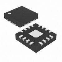
MAX5138BGTE+ Maxim Integrated Products, MAX5138BGTE+ Datasheet - Page 4

MAX5138BGTE+
Manufacturer Part Number
MAX5138BGTE+
Description
IC DAC 16BIT SGL 16-TQFN
Manufacturer
Maxim Integrated Products
Datasheet
1.MAX5139GTE.pdf
(17 pages)
Specifications of MAX5138BGTE+
Settling Time
5µs
Number Of Bits
16
Data Interface
DSP, I²C, MICROWIRE™, Parallel, QSPI™, SPI™
Number Of Converters
1
Voltage Supply Source
Analog and Digital
Operating Temperature
-40°C ~ 105°C
Mounting Type
Surface Mount
Package / Case
16-TQFN Exposed Pad
Interface Type
Serial (SPI, QSPI, Microwire, DSP)
Supply Voltage (max)
5.25 V
Supply Voltage (min)
2.7 V
Maximum Operating Temperature
+ 105 C
Mounting Style
SMD/SMT
Maximum Power Dissipation
1176.5 mW
Minimum Operating Temperature
- 40 C
Supply Current
1 mA
Lead Free Status / RoHS Status
Lead free / RoHS Compliant
Power Dissipation (max)
-
Lead Free Status / Rohs Status
Lead free / RoHS Compliant
Low-Power, Single, 16-/12-Bit,
Buffered Voltage-Output DACs
ELECTRICAL CHARACTERISTICS (continued)
(V
T
Figure 1. Serial-Interface Timing Diagram
Note 1: Static accuracy tested without load.
Note 2: Linearity is tested within 20mV of AGND and AVDD
Note 3: Codes above 2047 are guaranteed to be within ±9 LSB
Note 4: Gain and offset tested within 100mV of AGND and AVDD
Note 5: Guaranteed by design.
Note 6: Device draws current in excess of the specified supply current when a digital input is driven with a voltage of VI < DVDD - 0.6V
Note 7: Excess current from AVDD is 10mA when powered without DVDD. Excess current from DVDD is 1mA when powered without
Note 8: All timing specifications are with respect to the digital input and output thresholds.
Note 9: Maximum daisy-chain clock frequency is limited to 25MHz.
4
POWER REQUIREMENTS (Note 7)
Analog Supply Voltage Range
Digital Supply Voltage Range
Supply Current
Power-Down Supply Current
TIMING CHARACTERISTICS (Note 8) (Figure 1)
Serial-Clock Frequency
SCLK Pulse-Width High
SCLK Pulse-Width Low
CS Fall-to-SCLK Fall Setup Time
SCLK Fall-to CS-Rise Hold Time
DIN-to-SCLK Fall Setup Time
DIN-to-SCLK Fall Hold Time
SCLK Fall to READY Transition
CS Pulse-Width High
LDAC Pulse Width
A
AVDD
= T
_______________________________________________________________________________________
MIN
= 2.7V to 5.25V, V
or VI > 0.5V. At VI = 2.2V with DVDD = 5.25V, this current can be as high as 2mA. The SPI inputs are CMOS-input-level com-
patible. The 30MHz clock frequency cannot be guaranteed for a minimum signal swing.
AVDD.
to T
PARAMETER
MAX
, unless otherwise noted. Typical values are at T
X = DON'T CARE.
READY
SCLK
DIN
CS
DVDD
X
= 2.7V to 5.25V, V
C7
t
SYMBOL
LDACPWL
DVDD
AVDD
I
I
I
I
f
t
AVDD
DVDD
AVPD
DVPD
SCLK
t
t
t
CSW
t
t
t
CSS
CSH
t
SRL
CH
DH
CL
DS
C6
t
No load, all digital inputs at 0 or DVDD
No load, all digital inputs at 0 or DVDD
(Note 9)
CH
AVDD
C5
≥ V
,
DVDD
D3
allowing for gain and offset error.
24th FALLING EDGE OF SCLK
.
COMMAND EXECUTED ON
CONDITIONS
, V
.
A
t
DS
AGND
= +25°C.)
D2
t
DH
= 0, V
D1
REFI
t
SRL
= V
D0
AVDD
- 0.25V, C
MIN
2.7
2.7
13
13
10
33
33
0
8
5
2
X
t
CSW
OUT
TYP
0.2
0.1
1
1
= 200pF, R
AVDD
MAX
5.25
1.6
10
30
30
2
2
OUT
UNITS
= 10kΩ,
MHz
mA
µA
µA
ns
ns
ns
ns
ns
ns
ns
ns
ns
V
V


