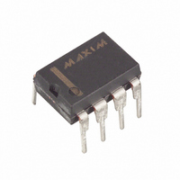
MAX535BCPA+ Maxim Integrated Products, MAX535BCPA+ Datasheet - Page 12

MAX535BCPA+
Manufacturer Part Number
MAX535BCPA+
Description
IC DAC V-OUT 13BIT 5V LP 8-DIP
Manufacturer
Maxim Integrated Products
Datasheet
1.MAX535BCUA.pdf
(16 pages)
Specifications of MAX535BCPA+
Settling Time
16µs
Number Of Bits
13
Data Interface
Serial
Number Of Converters
1
Voltage Supply Source
Single Supply
Power Dissipation (max)
552mW
Operating Temperature
0°C ~ 70°C
Mounting Type
Through Hole
Package / Case
8-DIP (0.300", 7.62mm)
Lead Free Status / RoHS Status
Lead free / RoHS Compliant
Figure 7 shows a method of connecting several
MAX535/MAX5351s. In this configuration, the clock and
the data bus are common to all devices and separate
chip-select lines are used for each IC.
For a unipolar output, the output voltage and the refer-
ence input have the same polarity. Figure 8 shows the
MAX535/MAX5351 unipolar output circuit, which is also
the typical operating circuit. Table 2 lists the unipolar
output codes.
For rail-to-rail output, see Figure 9. This circuit shows
the MAX535/MAX5351 with the output amplifier config-
ured with a closed-loop gain of +2 to provide 0V to 5V
full-scale range when a 2.5V reference is used. When
using the MAX5351 with a 1.25V reference, this circuit
provides a 0V to 2.5V full-scale range.
The MAX535/MAX5351 output can be configured for
bipolar operation using Figure 10’s circuit.
where NB is the numeric value of the DAC’s binary input
code. Table 3 shows digital codes (offset binary) and
the corresponding output voltage for Figure 10’s circuit.
Low-Power, 13-Bit Voltage-Output DACs
with Serial Interface
Figure 7. Multiple MAX535/MAX5351s Sharing Common DIN and SCLK Lines
12
__________Applications Information
______________________________________________________________________________________
SCLK
CS1
CS2
CS3
DIN
V
OUT
= V
REF
CS
SCLK
DIN
[(2NB / 8192) - 1]
MAX5351
MAX535
Unipolar Output
Bipolar Output
CS
SCLK
DIN
MAX5351
MAX535
In applications where the reference has AC-signal com-
ponents, the MAX535/MAX5351 have multiplying capa-
bility within the reference input range specifications.
Figure 11 shows a technique for applying a sine-wave
signal to the reference input where the AC signal is off-
set before being applied to REF. The reference voltage
must never be more negative than GND.
Table 2. Unipolar Code Table
1 1 1 1 1
1 0 0 0 0
1 0 0 0 0
0 1 1 1 1
0 0 0 0 0
0 0 0 0 0
MSB
DAC CONTENTS
1 1 1 1
0 0 0 0
0 0 0 0
1 1 1 1
0 0 0 0
0 0 0 0
CS
SCLK
DIN
LSB
1 1 1 1
0 0 0 1
0 0 0 0
1 1 1 1
0 0 0 1
0 0 0 0
MAX5351
MAX535
Using an AC Reference
+V
REF
ANALOG OUTPUT
+V
+V
+V
+V
REF
REF
4096
8192
REF
REF
TO OTHER
SERIAL DEVICES
0V
8192
4097
8192
4095
8192
8192
8191
1
V
REF
2


