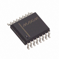
MAX536ACWE+ Maxim Integrated Products, MAX536ACWE+ Datasheet - Page 16

MAX536ACWE+
Manufacturer Part Number
MAX536ACWE+
Description
IC DAC 12BIT QUAD CALIB 16-SOIC
Manufacturer
Maxim Integrated Products
Datasheet
1.MAX536BCWE.pdf
(24 pages)
Specifications of MAX536ACWE+
Settling Time
3µs
Number Of Bits
12
Data Interface
Serial
Number Of Converters
4
Voltage Supply Source
Dual ±
Power Dissipation (max)
762mW
Operating Temperature
0°C ~ 70°C
Mounting Type
Surface Mount
Package / Case
16-SOIC (0.300", 7.5mm Width)
Lead Free Status / RoHS Status
Lead free / RoHS Compliant
Calibrated, Quad, 12-Bit
Voltage-Output DACs with Serial Interface
When daisy-chaining MAX536s, the delay from CS
low to SCK high (t
where t
(R
t
equation:
where V
connected.
16
Table 1. Serial-Interface Programming Commands
CSS
“X” = Don’t Care. LDAC provides true latch control: when LDAC is low, the DAC registers are transparent; when LDAC is high,
the DAC registers are latched.
A1
p
X
X
0
0
1
1
0
0
1
1
0
1
1
0
0
1
1
) and the load capacitance (C) at SDO. For t
is simply t
______________________________________________________________________________________
RC
PULL-UP
A0
X
0
1
0
1
0
1
0
1
0
1
1
0
0
1
0
1
is the time constant of the external pull-up resistor
t
RC
16-BIT SERIAL WORD
DV
C1
= R
0
0
0
0
1
1
1
1
0
0
1
1
1
X
X
X
X
is the voltage to which the pull-up resistor is
CSS
+ t
t
p
TR
DS
) must be the greater of:
(C)
C0
1
1
1
1
1
1
1
1
0
0
0
0
0
1
1
1
1
+ t
. Calculate t
t
RC
DV
[
ln
12-bit DAC data
12-bit DAC data
12-bit DAC data
12-bit DAC data
12-bit DAC data
12-bit DAC data
12-bit DAC data
12-bit DAC data
12-bit DAC data
X X X X X X X X X X X X
X X X X X X X X X X X X
X X X X X X X X X X X X
X X X X X X X X X X X X
12-bit DAC data
12-bit DAC data
12-bit DAC data
12-bit DAC data
or
+ t
+ t
(
DS
DS
V
D11…D0
PULL-UP
- t
RC
V
CSW
PULL-UP
from the following
- 2.4V
RC
< 20ns,
)
LDAC
]
1
1
1
1
1
1
1
1
X
X
1
X
X
0
0
0
0
Additionally, when daisy-chaining devices, the maximum
clock frequency is limited to:
For example, with t
R
8.7MHz.
Figure 9 shows an alternate method of connecting several
MAX536/MAX537s. In this configuration, the data bus is
common to all devices; data is not shifted through a
daisy-chain. More I/O lines are required in this configu-
ration because a dedicated chip-select input (CS) is
required for each IC.
Load DAC A input register; DAC output unchanged.
Load DAC B input register; DAC output unchanged.
Load DAC C input register; DAC output unchanged.
Load DAC D input register; DAC output unchanged.
Load input register A; all DAC registers updated.
Load input register B; all DAC registers updated.
Load input register C; all DAC registers updated.
Load input register D; all DAC registers updated.
Load all DACs from shift register.
No operation (NOP)
Update all DACs from their respective input registers.
Mode 1 (default condition at power-up), DOUT clocked out on
SCK’s rising edge. All DACs updated from their respective
input registers.
Mode 0, DOUT clocked out on SCK’s falling edge. All DACs
updated from their respective input registers.
Load DAC A input register; DAC A is immediately updated.
Load DAC B input register; DAC B is immediately updated.
Load DAC C input register; DAC C is immediately updated.
Load DAC D input register; DAC D is immediately updated.
p
= 1k and C = 30pF), the maximum clock frequency is
f
SCK
(max) = ——————————————
RC
2 (t
FUNCTION
= 23ns (5V ±10% supply with
DO
+ t
RC
1
- 38ns + t
DS
)


