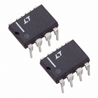
LTC1661IN8 Linear Technology, LTC1661IN8 Datasheet - Page 4

LTC1661IN8
Manufacturer Part Number
LTC1661IN8
Description
IC D/A CONV 10BIT MICRPWR 8-DIP
Manufacturer
Linear Technology
Datasheet
1.LTC1661CMS8PBF.pdf
(14 pages)
Specifications of LTC1661IN8
Settling Time
30µs
Number Of Bits
10
Data Interface
Serial
Number Of Converters
2
Voltage Supply Source
Single Supply
Power Dissipation (max)
260µW
Operating Temperature
-40°C ~ 85°C
Mounting Type
Through Hole
Package / Case
8-DIP (0.300", 7.62mm)
Lead Free Status / RoHS Status
Contains lead / RoHS non-compliant
LTC1661
TIMING CHARACTERISTICS
Note 1: Stresses beyond those listed under Absolute Maximum Ratings
may cause permanent damage to the device. Exposure to any Absolute
Maximum Rating condition for extended periods may affect device
reliability and lifetime.
Note 2: Nonlinearity and monotonicity are defined from code 20 to code
1023 (full scale). See Applications Information.
TIMING DIAGRAM
SYMBOL
V
t
t
t
t
t
t
t
t
t
4
range, otherwise specifications are at T
1
2
3
4
5
6
7
9
11
CC
= 2.7V to 5.5V
CS/LD
SCK
D
IN
PARAMETER
D
D
SCK High Time
SCK Low Time
CS/LD Pulse Width
LSB SCK High to CS/LD High
CS/LD Low to SCK High
SCK Low to CS/LD Low
CS/LD High to SCK Positive Edge
SCK Frequency
IN
IN
Valid to SCK Setup
Valid to SCK Hold
t
5
t
9
t
7
A
= 25°C.
t
1
A3
t
2
CONDITIONS
(Note 6)
(Note 6)
(Note 6)
(Note 6)
(Note 6)
(Note 6)
(Note 6)
(Note 6)
(Note 6)
Square Wave (Note 6)
The
l
denotes the specifications which apply over the full operating temperature
A2
t
3
Note 3: Digital inputs at 0V or V
Note 4: Load is 10kΩ in parallel with 100pF.
Note 5: V
i.e., codes k = 102 and k = 922.
Note 6: Guaranteed by design and not subject to test.
t
4
A1
CC
= V
REF
= 5V. DAC switched between 0.1V
X1
l
l
l
l
l
l
l
l
l
l
CC
MIN
100
60
50
50
50
30
30
0
0
.
X0
t
6
TYP
1661 TD
t
11
FS
MAX
and 0.9V
10
FS
,
UNITS
1661fa
MHz
ns
ns
ns
ns
ns
ns
ns
ns
ns


