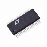
LTC1821-1BCGW#TR Linear Technology, LTC1821-1BCGW#TR Datasheet - Page 9

LTC1821-1BCGW#TR
Manufacturer Part Number
LTC1821-1BCGW#TR
Description
IC D/A CONV 16BIT PRECISE 36SSOP
Manufacturer
Linear Technology
Datasheet
1.LTC1821-1BCGWPBF.pdf
(16 pages)
Specifications of LTC1821-1BCGW#TR
Settling Time
2µs
Number Of Bits
16
Data Interface
Parallel
Number Of Converters
1
Voltage Supply Source
Single Supply
Operating Temperature
0°C ~ 70°C
Mounting Type
Surface Mount
Package / Case
36-SSOP
Lead Free Status / RoHS Status
Contains lead / RoHS non-compliant
Power Dissipation (max)
-
Other names
LTC1821-1BCGWTR
Available stocks
Company
Part Number
Manufacturer
Quantity
Price
APPLICATIONS
TI I G DIAGRA
Description
The LTC1821 is a 16-bit voltage output DAC with a full
parallel 16-bit digital interface. The device can operate
from 5V and 15 supplies and provides both unipolar 0V
to – 10V or 0V to 10V and bipolar 10V output ranges from
a 10V or –10V reference input. Additionally, the power
supplies for the LTC1821 can go as low as 4.5V and 4.5V.
In this case for a 2.5V or – 2.5V reference, the output range
is 0V to – 2.5V, 0V to 2.5V and 2.5V. The LTC1821 has
three additional precision resistors on chip for bipolar
operation. Refer to the block diagram regarding the fol-
lowing description.
The 16-bit DAC consists of a precision R-2R ladder for the
13 LSBs. The three MSBs are decoded into seven seg-
ments of resistor value R. Each of these segments and the
R-2R ladder carries an equally weighted current of one
eighth of full scale. The feedback resistor R
4-quadrant resistor R
resistors R1 and R2 have a magnitude of R/4. R1 and R2
together with an external op amp (see Figure 2) inverts the
reference input voltage and applies it to the 16-bit DAC
input REF, in 4-quadrant operation. The REF pin presents
a constant input impedance of R/8 in unipolar mode and
R/12 in bipolar mode.
W
U
U
OFS
INFORMATION
have a value of R/4. 4-quadrant
U
W
DATA
CLR
WR
LD
W
U
FB
t
t
WR
DS
and
t
DH
t
The LTC1821 contains an onboard precision high speed
amplifier. This amplifier together with the feedback resis-
tor (R
the DAC’s current output. The amplifier has very low noise,
offset, input bias current and settles in less than 2 s to
0.0015% for a 10V step. It can sink and source 22mA
( 15V) typically and can drive a 300pF capacitive load. An
added feature of these devices, especially for waveform
generation, is a proprietary deglitcher that reduces glitch
impulse to below 2nV-s over the DAC output voltage range.
Digital Section
The LTC1821 has a 16-bit wide full parallel data bus input.
The device is double-buffered with two 16-bit registers.
The double-buffered feature permits the update of several
DACs simultaneously. The input register is loaded directly
from a 16-bit microprocessor bus when the WR pin is
brought to a logic low level. The second register (DAC
register) is updated with the data from the input register
when the LD signal is brought to a logic high. Updating the
DAC register updates the DAC output with the new data. To
make both registers transparent in flowthrough mode, tie
WR low and LD high. However, this defeats the deglitcher
operation and output glitch impulse may increase. The
deglitcher is activated on the rising edge of the LD pin. The
LWD
FB
) form a precision current-to-voltage converter for
t
LD
t
CLR
1821 TD
LTC1821
9


