AD7533JN Analog Devices Inc, AD7533JN Datasheet - Page 2
AD7533JN
Manufacturer Part Number
AD7533JN
Description
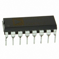
IC DAC 10BIT MULTIPLYING 16-DIP
Manufacturer
Analog Devices Inc
Datasheet
1.AD7533KRZ.pdf
(12 pages)
Specifications of AD7533JN
Data Interface
Parallel
Settling Time
600ns
Rohs Status
RoHS non-compliant
Number Of Bits
10
Number Of Converters
1
Voltage Supply Source
Single Supply
Power Dissipation (max)
30mW
Operating Temperature
-40°C ~ 85°C
Mounting Type
Through Hole
Package / Case
16-DIP (0.300", 7.62mm)
Resolution (bits)
10bit
Digital Ic Case Style
DIP
No. Of Pins
16
Operating Temperature Range
-40°C To +85°C
Update Rate
1.7MSPS
Lead Free Status / RoHS Status
Contains lead / RoHS non-compliant
Available stocks
Company
Part Number
Manufacturer
Quantity
Price
Company:

Part Number:
AD7533JN
Manufacturer:
AD
Quantity:
5 510
Part Number:
AD7533JN
Manufacturer:
ADI/亚德诺
Quantity:
20 000
Part Number:
AD7533JNZ
Manufacturer:
ADI/亚德诺
Quantity:
20 000


AD7533
TABLE OF CONTENTS
Features .............................................................................................. 1
Applications....................................................................................... 1
General Description ......................................................................... 1
Functional Block Diagram .............................................................. 1
Revision History ............................................................................... 2
Specifications..................................................................................... 3
Absolute Maximum Ratings............................................................ 4
Terminology ...................................................................................... 5
Pin Configurations and Function Descriptions ........................... 6
REVISION HISTORY
3/07—Rev. B to Rev. C
Changes to Table 1............................................................................ 3
Changes to Table 2............................................................................ 4
Changes to Figure 13, Figure 14, and Figure 17 ........................... 9
Updated Outline Dimensions ....................................................... 10
Changes to Ordering Guide .......................................................... 12
1/06—Rev. A to Rev. B
Updated Format..................................................................Universal
Changes to Absolute Maximum Ratings ....................................... 4
Added Pin Configurations
and Function Descriptions Section................................................ 6
Updated Outline Dimensions ....................................................... 10
Changes to Ordering Guide .......................................................... 12
ESD Caution.................................................................................. 4
Rev. C | Page 2 of 12
Circuit Description............................................................................7
Operation............................................................................................8
Applications........................................................................................9
Outline Dimensions ....................................................................... 10
3/04—Rev. 0 to Rev. A
Changes to Specifications.................................................................2
Changes to Absolute Maximum Ratings........................................3
Changes to Ordering Guide .............................................................3
Updated Outline Dimensions..........................................................7
General Circuit Information........................................................7
Equivalent Circuit Analysis .........................................................7
Unipolar Binary Code ..................................................................8
Bipolar (Offset Binary) Code.......................................................8
Ordering Guide .......................................................................... 12
Related parts for AD7533JN
Image
Part Number
Description
Manufacturer
Datasheet
Request
R

Part Number:
Description:
±1.7g Dual-Axis IMEMS Accelerometer Evaluation Board
Manufacturer:
Analog Devices Inc
Datasheet:

Part Number:
Description:
Inertial Sensor Evaluation System
Manufacturer:
Analog Devices Inc
Datasheet:
Part Number:
Description:
Manufacturer:
Analog Devices Inc
Datasheet:
Part Number:
Description:
Manufacturer:
Analog Devices Inc
Datasheet:
Part Number:
Description:
Manufacturer:
Analog Devices Inc
Datasheet:
Part Number:
Description:
Manufacturer:
Analog Devices Inc
Datasheet:
Part Number:
Description:
Manufacturer:
Analog Devices Inc
Datasheet:
Part Number:
Description:
Manufacturer:
Analog Devices Inc
Datasheet:
Part Number:
Description:
Manufacturer:
Analog Devices Inc
Datasheet:
Part Number:
Description:
Manufacturer:
Analog Devices Inc
Datasheet:
Part Number:
Description:
Manufacturer:
Analog Devices Inc
Datasheet:
Part Number:
Description:
Manufacturer:
Analog Devices Inc
Datasheet:
Part Number:
Description:
Manufacturer:
Analog Devices Inc
Datasheet: