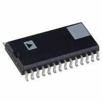
AD9760AR50 Analog Devices Inc, AD9760AR50 Datasheet - Page 4

AD9760AR50
Manufacturer Part Number
AD9760AR50
Description
IC DAC 10BIT 50MSPS 28-SOIC
Manufacturer
Analog Devices Inc
Series
TxDAC®r
Datasheet
1.AD9760ARUZ.pdf
(23 pages)
Specifications of AD9760AR50
Rohs Status
RoHS non-compliant
Settling Time
35ns
Number Of Bits
10
Number Of Converters
1
Voltage Supply Source
Analog and Digital
Power Dissipation (max)
175mW
Operating Temperature
-40°C ~ 85°C
Mounting Type
Surface Mount
Package / Case
28-SOIC (7.5mm Width)
Resolution (bits)
10bit
Input Channel Type
Parallel
Digital Ic Case Style
SOIC
No. Of Pins
28
Operating Temperature Range
-40°C To +85°C
Msl
MSL 3 - 168 Hours
Data Interface
Parallel
For Use With
AD9760-EBZ - BOARD EVAL FOR AD9760
Lead Free Status / RoHS Status
Contains lead / RoHS non-compliant
Available stocks
Company
Part Number
Manufacturer
Quantity
Price
Part Number:
AD9760AR50
Manufacturer:
ADI/亚德诺
Quantity:
20 000
AD9760
DIGITAL SPECIFICATIONS
Parameter
DIGITAL INPUTS
Specification subject to change without notice.
ABSOLUTE MAXIMUM RATINGS*
Parameter
AVDD
DVDD
ACOM
AVDD
CLOCK, SLEEP
Digital Inputs
I
COMP1, COMP2
REFIO, FSADJ
REFLO
Junction Temperature
Storage Temperature
Lead Temperature
*Stresses above those listed under Absolute Maximum Ratings may cause perma-
CAUTION
ESD (electrostatic discharge) sensitive device. Electrostatic charges as high as 4000 V readily
accumulate on the human body and test equipment and can discharge without detection.
Although the AD9760 features proprietary ESD protection circuitry, permanent damage may
occur on devices subjected to high energy electrostatic discharges. Therefore, proper ESD
precautions are recommended to avoid performance degradation or loss of functionality.
OUTA
nent damage to the device. This is a stress rating only; functional operation of the
device at these or any other conditions above those indicated in the operational
sections of this specification is not implied. Exposure to absolute maximum
ratings for extended periods may effect device reliability.
(10 sec)
Logic “1” Voltage @ DVDD = +5 V
Logic “1” Voltage @ DVDD = +3 V
Logic “0” Voltage @ DVDD = +5 V
Logic “0” Voltage @ DVDD = +3 V
Logic “1” Current
Logic “0” Current
Input Capacitance
Input Setup Time (t
Input Hold Time (t
Latch Pulsewidth (t
, I
OUTB
H
LPW
S
With
Respect to
ACOM
DCOM
DCOM
DVDD
DCOM
DCOM
ACOM
ACOM
ACOM
ACOM
)
)
)
DB0–DB9
Min
–0.3
–0.3
–0.3
–6.5
–0.3
–0.3
–1.0
–0.3
–0.3
–0.3
–65
I
OUTA
CLOCK
I
OUTB
(T
OR
MIN
Max
+6.5
+6.5
+0.3
+6.5
DVDD + 0.3
DVDD + 0.3
AVDD + 0.3
AVDD + 0.3
AVDD + 0.3
+0.3
+150
+150
+300
to T
MAX
, AVDD = +5 V, DVDD = +5 V, I
Figure 1. Timing Diagram
t
S
Units
V
V
V
V
V
V
V
V
V
V
°C
°C
°C
t
PD
–4–
0.1%
Model
AD9760AR
AD9760ARU
AD9760AR50
AD9760ARU50 –40°C to +85°C
AD9760-EB
THERMAL CHARACTERISTICS
Thermal Resistance
28-Lead 300 mil (7.5 mm) SOIC
28-Lead 170 mil (4.4 mm) TSSOP
t
t
θ
θ
θ
θ
LPW
ST
JA
JC
JA
JC
Min
3.5
2.1
–10
–10
2.0
1.5
3.5
= 71.4°C/W
= 97.9°C/W
= 23°C/W
= 14.0°C/W
t
H
OUTFS
0.1%
= 20 mA unless otherwise noted)
Temperature
Range
–40°C to +85°C
–40°C to +85°C
–40°C to +85°C
Evaluation Board
5
3
Typ
0
0
5
ORDERING GUIDE
WARNING!
Max
1.3
0.9
+10
+10
Package
Descriptions
28-Lead 300 mil R-28
SOIC
28-Lead 170 mil RU-28
TSSOP
28-Lead 300 mil R-28
SOIC
28-Lead 170 mil RU-28
TSSOP
ESD SENSITIVE DEVICE
V
V
V
V
Units
µA
µA
pF
ns
ns
ns
Package
Options
REV. B


