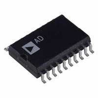
AD7849AR-REEL Analog Devices Inc, AD7849AR-REEL Datasheet - Page 13

AD7849AR-REEL
Manufacturer Part Number
AD7849AR-REEL
Description
IC DAC 16BIT SRL INP 20-SOIC
Manufacturer
Analog Devices Inc
Datasheet
1.AD7849BRZ.pdf
(20 pages)
Specifications of AD7849AR-REEL
Rohs Status
RoHS non-compliant
Settling Time
7µs
Number Of Bits
16
Data Interface
Serial
Number Of Converters
1
Voltage Supply Source
Analog and Digital, Dual ±
Power Dissipation (max)
100mW
Operating Temperature
-40°C ~ 85°C
Mounting Type
Surface Mount
Package / Case
20-SOIC (7.5mm Width)
Serial Data Loading Format (Daisy-Chain Mode)
By connecting DCEN high, daisy-chain mode is enabled. This
mode of operation is designed for multiDAC systems where
several
internal gating circuitry on SCLK is disabled, and a serial data
output facility is enabled. The internal gating signal is permanently
active (low) so that the SCLK signal is continuously applied to
the input shift register when SYNC is low. The data is clocked
into the register on each falling SCLK edge after SYNC goes low. If
more than 16 clock pulses are applied, the data ripples out of the
shift register and appears on the SDOUT line. By connecting this
line to the SDIN input on the next
multiDAC interface can be constructed. Sixteen SCLK pulses
are required for each DAC in the system. Therefore, the total
number of clock cycles must equal 16 × N, where N is the total
number of devices in the chain. When the serial transfer to all
devices is complete,
further data from being clocked into the input register.
A continuous SCLK source can be used if SYNC is held low for
the correct number of clock cycles. Alternatively, a burst clock
containing the exact number of clock cycles can be used and
SYNC taken high some time later.
When the transfer to all input registers is complete, a common
LDAC signal updates all DAC latches with the data in each input
register. All analog outputs are therefore updated simultaneously,
5 μs after the falling edge of LDAC .
AD7849s
NOTES
1. DCEN IS TIED PERMANENTLY HIGH.
(AD7849B/C)
(AD7849B/C)
LDAC, CLR
(AD7849A)
(AD7849A)
BIN/COMP
SDOUT
SDOUT
SCLK
SYNC
can be connected in cascade. In this mode, the
SDIN
SDIN
SYNC is taken high, which prevents any
DB13 (N)
DB15 (N)
t
2
AD7849
DB0 (N)
in the chain, a
Figure 18. Timing Diagram (Daisy-Chain Mode)
DB0 (N)
t
1
t
t
6
6
Rev. C | Page 13 of 20
DB13 (N)
DB15 (N)
t
t
(N + 1)
(N + 1)
DB13
4
DB15
4
t
t
5
5
DB0 (N)
(N + 1)
DB0
Clear Function ( CLR )
The clear function bypasses the input shift register and loads
the DAC latch with all 0s. It is activated by taking CLR low. In
all ranges, except the offset binary bipolar range (–5 V to +5 V),
the output voltage is reset to 0 V. In the offset binary bipolar
range, the output is set to V
separate from the automatic power-on reset feature of the device.
APPLYING THE AD7849
Power Supply Sequencing and Decoupling
In the AD7849, V
If this happens, then an internal diode is turned on, and it produces
latch-up in the device. Care should be taken to employ the
following power supply sequence: V
systems where it is possible to have an incorrect power sequence
(for example, if V
the circuit shown in Figure 19 can be used to ensure that the
Absolute Maximum Ratings are not exceeded.
DB0 (N)
(N + 1)
DB0
t
3
CC
Figure 19. Power Supply Protection
CC
1N4148
is greater than 0.4 V while V
should not exceed V
V
V
DD
DD
REF–
AD7849
. This clear function is distinct and
SD103C
1N5711
1N5712
t
DD,
V
V
7
CC
CC
V
DD
SS,
and then V
by more than 0.4 V.
DD
is still 0 V),
AD7849
CC
. In


