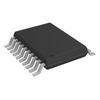
DAC8562FRU Analog Devices Inc, DAC8562FRU Datasheet - Page 11

DAC8562FRU
Manufacturer Part Number
DAC8562FRU
Description
IC DAC 12BIT PARALLEL 5V 20TSSOP
Manufacturer
Analog Devices Inc
Datasheet
1.DAC8562FSZ.pdf
(16 pages)
Specifications of DAC8562FRU
Rohs Status
RoHS non-compliant
Settling Time
16µs
Number Of Bits
12
Data Interface
Parallel
Number Of Converters
1
Voltage Supply Source
Single Supply
Power Dissipation (max)
30mW
Operating Temperature
-40°C ~ 85°C
Mounting Type
Surface Mount
Package / Case
20-TSSOP
REV. A
Bipolar Output Operation
Although the DAC8562 has been designed for single supply op-
eration, bipolar operation is achievable using the circuit illus-
trated in Figure 33. The circuit uses a single supply, rail-to-rail
OP295 op amp and the DAC’s internal +2.5 V reference to gen-
erate the –2.5 V reference required to level-shift the DAC out-
put voltage. The circuit has been configured to provide an
output voltage in the range –5 V V
complementary offset binary. Although each DAC LSB corre-
sponds to 1 mV, each output LSB has been scaled to 2.44 mV.
Table IV provides the relationship between the digital codes and
output voltage.
The transfer function of the circuit is given by:
and, for the circuit values shown, becomes:
Hexadecimal Number
in DAC Register
FFF
801
800
7FF
000
To maintain monotonicity and accuracy, R1, R2, R4, R5, and
R6 should be selected to match within 0.01% and must all be of
the same (preferably metal foil) type to assure temperature coef-
ficient matching. Mismatching between R1 and R2 causes offset
and gain errors while an R4 to R1 and R2 mismatch yields gain
errors.
For applications that do not require high accuracy, the circuit il-
lustrated in Figure 34 can also be used to generate a bipolar
output voltage. In this circuit, only one op amp is used and no
potentiometers are used for offset and gain trim The output
voltage is coded in offset binary and is given by:
V
O
CLR
V
CE
1 mV
O
DATA
Table IV. Bipolar Code Table
–2.44 mV
16
15
10µF
Digital Code
DGND
DAC-8562
10
Decimal Number
in DAC Register
4095
2049
2048
2047
0
+5V
V
20
DD
REFOUT
AGND
12
V
0.1µF
Digital Code 5 V
OUT
13
14
OUT
R4
R1
+5 V and is coded in
10k
R5
2.5
Figure 33. Bipolar Output Operation
Analog Output
Voltage (V)
–4 9976
–2.44E–3
0
+2.44E–3
+5
10k
R1
6
5
10k
R4
R2
R6
A2
12.7k
–2.5V
R2
7
–11–
ZERO SCALE
For the 2 5 V output range and the circuit values shown in the
table, the transfer equation becomes:
Similarly, for the 5 V output range, the transfer equation be-
comes:
Note that, for 5 V output voltage operation, R5 is required as a
pull-down for REFOUT. Or, REFOUT can be buffered by an
op amp configured as a follower that can source and sink cur-
rent.
ADJUST
10k
P1
CLR
CE
R3
247k
V
DATA
Figure 34. Bipolar Output Operation Without
Trim Version 1
O
16
15
1 mV
0.1µF
V
A1, A2 = 1/2 OP-295
V
DGND
O
DAC-8562
O
10
V
+5V
1.22 mV
20
DD
23.7k
REFOUT
Digital Code
2.44 mV
3
2
R4
AGND
12
– REFOUT
V
A1
OUT
+5V
–5V
8
4
14
V
RANGE
±2.5V
±5V
13
OUT
1
500
P2
Digital Code – 2.5 V
Digital Code – 5 V
FULL SCALE
ADJUST
R5
4.99k
R1
10k
10k
R3
R1
R3 R4
R2
R1
R4
–5V
R2
10k
20k
R4
2
3
V
A1 = 1/2 OP-295
R3
10k
10k
A1
DAC8562
O
R2
+5V
–5V
4
+5V
8
1
R4
15.4k + 274
43.2k + 499
1
R2
R1
V
O


