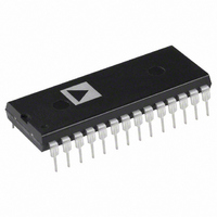
DAC8408FP Analog Devices Inc, DAC8408FP Datasheet - Page 9

DAC8408FP
Manufacturer Part Number
DAC8408FP
Description
IC DAC 8BIT QUAD W/MEMORY 28-DIP
Manufacturer
Analog Devices Inc
Datasheet
1.DAC8408FSZ-REEL.pdf
(16 pages)
Specifications of DAC8408FP
Rohs Status
RoHS non-compliant
Settling Time
190ns
Number Of Bits
8
Data Interface
Parallel
Number Of Converters
4
Voltage Supply Source
Single Supply
Operating Temperature
-40°C ~ 85°C
Mounting Type
Through Hole
Package / Case
28-DIP (0.600", 15.24mm)
Power Dissipation (max)
-
Available stocks
Company
Part Number
Manufacturer
Quantity
Price
Company:
Part Number:
DAC8408FP
Manufacturer:
INFINEON
Quantity:
683
Part Number:
DAC8408FP
Manufacturer:
ADI/亚德诺
Quantity:
20 000
Company:
Part Number:
DAC8408FPC
Manufacturer:
TI
Quantity:
8 831
Company:
Part Number:
DAC8408FPC
Manufacturer:
Analog Devices Inc
Quantity:
10 000
Company:
Part Number:
DAC8408FPZ
Manufacturer:
SUPLET
Quantity:
25
DIGITAL SECTION
Figure 5 shows the digital input/output structure for one bit.
The digital WR, WR, and RD controls shown in the figure are
internally generated from the external A/B, R/W, DS1, and DS2
signals. The combination of these signals decide which DAC is
selected. The digital inputs are CMOS inverters, designed such
that TTL input levels (2.4 V and 0.8 V) are converted into
CMOS logic levels. When the digital input is in the region of 1.2 V
to 1.8 V, the input stages operate in their linear region and draw
current from the +5 V supply (see Typical Supply Current vs.
Logic Level curve on page 6). It is recommended that the digital
input voltages be as close to V
order to minimize supply currents. This allows maximum sav-
ings in power dissipation inherent with CMOS devices. The
three-state readback digital output drivers (in the active mode)
provide TTL-compatible digital outputs with a fan-out of one
TTL load. The three state digital readback leakage-current is
typically 5 nA.
REV. A
Figure 4. Equivalent DAC Circuit (AII Digital Inputs LOW)
Figure 5. Digital Input/Output Structure
DD
and DGND as is practical in
–9–
INTERFACE LOGIC SECTION
DAC Operating Modes
• All DACs in HOLD MODE.
• DAC A, B, C, or D individually selected (WRITE MODE).
• DAC A, B, C, or D individually selected (READ MODE).
• DACs A and C simultaneously selected (WRITE MODE).
• DACs B and D simultaneously selected (WRITE MODE).
DAC Selection: Control inputs, DS1, DS2, and A/B select
which DAC can accept data from the input port (see Mode Se-
lection Table).
Mode Selection: Control inputs DS and R/W control the oper-
ating mode of the selected DAC.
Write Mode: When the control inputs DS and R/W are both
low, the selected DAC is in the write mode. The input data
latches of the selected DAC are transparent, and its analog out-
put responds to activity on the data inputs DB0–DB7.
Hold Mode: The selected DAC latch retains the data that was
present on the bus line just prior to DS or R/W going to a high
state. All analog outputs remain at the values corresponding to
the data in their respective latches.
Read Mode: When DS is low and R/W is high, the selected
DAC is in the read mode, and the data held in the appropriate
latch is put back onto the data bus.
DS1
L
L
H
H
L
L
H
H
L
L
H
L
L
L = Low State, H = High State, X = Irrelevant
Control Logic
DS2 A/B
H
H
L
L
H
H
L
L
L
L
H
L
L
H
L
H
L
H
L
H
L
H
L
X
H
L
MODE SELECTION TABLE
R/W
L
L
L
L
H
H
H
H
L
L
X
H
H
Mode
WRITE
WRITE
WRITE
WRITE
READ
READ
READ
READ
WRITE
WRITE
HOLD
HOLD
HOLD
DAC8408
DAC
A
B
C
D
A
B
C
D
A&C
B&D
A/B/C/D
A/B/C/D
A/B/C/D


