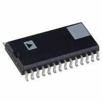
DAC8408FS Analog Devices Inc, DAC8408FS Datasheet - Page 10

DAC8408FS
Manufacturer Part Number
DAC8408FS
Description
IC DAC 8BIT QUAD W/MEMORY 28SOIC
Manufacturer
Analog Devices Inc
Datasheet
1.DAC8408FSZ-REEL.pdf
(16 pages)
Specifications of DAC8408FS
Rohs Status
RoHS non-compliant
Settling Time
190ns
Number Of Bits
8
Data Interface
Parallel
Number Of Converters
4
Voltage Supply Source
Single Supply
Operating Temperature
-40°C ~ 85°C
Mounting Type
Surface Mount
Package / Case
28-SOIC (7.5mm Width)
Power Dissipation (max)
-
Available stocks
Company
Part Number
Manufacturer
Quantity
Price
Part Number:
DAC8408FSZ
Manufacturer:
ADI/亚德诺
Quantity:
20 000
DAC8408
BASIC APPLICATIONS
Some basic circuit configurations are shown in Figures 6 and 7.
Figure 6 shows the DAC8408 connected in a unipolar configu-
ration (2-Quadrant Multiplication), and Table I shows the Code
Table. Resistors R1, R2, R3, and R4 are used to trim full scale
output. Full-scale output voltage = V
or V
ture coefficient (approximately 50 ppm/ C) resistors or trim-
mers should be selected if used. Full scale can also be adjusted
using V
R4. In many applications, R1 through R4 are not required, and
the maximum gain error will then be that of the DAC.
Each DAC exhibits a variable output resistance that is code-
dependent. This produces a code-dependent, differential non-
linearity term at the amplifier’s output which can have a maxi-
mum value of 0.67
ential nonlinearity term adds to the R-2R resistor ladder differ-
ential-nonlinearity; the output may no longer be monotonic. To
maintain monotonicity and minimize gain and linearity errors, it
is recommended that the op amp offset voltage be adjusted to
less than 10% of 1 LSB (1 LSB = 2
or less than 3.9 mV over the operating temperature range. Zero-
scale output voltage (with all digital inputs low) may be adjusted
using the op amp offset adjustment. Capacitors C1, C2, C3,
and C4 provide phase compensation and help prevent overshoot
and ringing when using high speed op amps.
Figure 7 shows the recommended circuit configuration for the
bipolar operation (4-quadrant multiplication), and Table II shows
the Code Table. Trimmer resistors R17, R18, R19, and R20
REF
REF
(255/256) with all digital inputs high. Low tempera-
voltage. This will eliminate resistors R1, R2, R3, and
the amplifier’s offset voltage. This differ-
Figure 6. Quad DAC Unipolar Operation (2-Quadrant Multiplication)
–8
REF
V
–1 LSB = V
REF
or 1/256
REF
V
(1–2
REF
),
–8
)
–10–
DAC Data Input
MSB
1 1 1 1 1 1 1 1
1 0 0 0 0 0 0 1
1 0 0 0 0 0 0 0
0 1 1 1 1 1 1 1
0 0 0 0 0 0 0 1
0 0 0 0 0 0 0 0
NOTE
1 LSB = (2
are used only if gain error adjustments are required and range
between 50
will range betwen 50
is essential that resistor pairs R9–R13, R10–R14, R11–R15,
R12–R16 are matched both in value and tempco. They should
be within 0.01%; wire wound or metal foil types are preferred
for best temperature coefficient matching. The circuits of Figure
6 and 7 can either be used as a fixed reference D/A converter, or
as an attenuator with an ac input voltage.
Table I. Unipolar Binary Code Table (Refer to Figure 6)
–8
) (V
REF
and 1000 . Resistors R21, R22, R23, and R24
LSB
) =
256
1
(V
and 500 . If these resistors are used, it
REF
)
Analog Output
–V
–V
–V
–V
–V
–V
REF
REF
REF
REF
REF
REF
129
127
255
256
256
128
256
256
256
256
1
0
=
= 0
–V
2
IN
REV. A


