AD7837AQ Analog Devices Inc, AD7837AQ Datasheet - Page 5
AD7837AQ
Manufacturer Part Number
AD7837AQ
Description
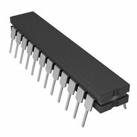
IC DAC 12BIT DUAL MULT 24-CDIP
Manufacturer
Analog Devices Inc
Datasheet
1.AD7837ARZ.pdf
(12 pages)
Specifications of AD7837AQ
Rohs Status
RoHS non-compliant
Settling Time
4µs
Number Of Bits
12
Data Interface
Parallel
Number Of Converters
2
Voltage Supply Source
Dual ±
Power Dissipation (max)
210mW
Operating Temperature
-40°C ~ 85°C
Mounting Type
Through Hole
Package / Case
24-CDIP (0.300", 7.62mm)


Pin
11
12
13
14
15
16
17
18
19
10
11
12
13
14–24
DB10–DB0
Mnemonic
CSA
CSB
V
V
AGNDA
V
V
AGNDB
V
V
DGND
DB11
WR
REFA
OUTA
DD
SS
OUTB
REFB
AD7837 PIN CONFIGURATION
AGNDA
AGNDB
V
V
V
V
DGND
R
OUTA
OUTB
R
REFA
REFB
AD7847 PIN FUNCTION DESCRIPTION (DIP AND SOIC PIN NUMBERS)
V
V
FBA
FBB
CS
DD
SS
DIP AND SOIC
Description
Chip Select Input for DAC A. Active low logic input. DAC A is selected when this input is low.
Chip Select Input for DAC B. Active low logic input. DAC B is selected when this input is low.
Reference Input Voltage for DAC A. This may be an ac or dc signal.
Analog Output Voltage from DAC A.
Analog Ground for DAC A.
Positive Power Supply.
Negative Power Supply.
Analog Ground for DAC B.
Analog Output Voltage from DAC B.
Reference Input Voltage for DAC B. This may be an ac or dc signal.
Digital Ground.
Data Bit 11 (MSB).
Write Input. WR is a positive edge triggered input which is used in conjunction with CSA and CSB
to write data to the DAC latches.
Data Bit 10 to Data Bit 0 (LSB).
12
10
11
1
2
3
4
5
6
7
8
9
(Not to Scale)
AD7837
TOP VIEW
24
23
22
21
20
19
18
17
16
15
14
13
DB0
DB1
DB2
DB3
DB4
DB5
DB6
DB7
A0
A1
LDAC
WR
AD7847 PIN CONFIGURATION
AGNDA
AGNDB
V
V
V
V
DGND
DB11
OUTA
OUTB
REFA
REFB
CSA
CSB
V
V
DD
SS
DIP AND SOIC
12
10
11
1
2
3
4
5
6
7
8
9
(Not to Scale)
AD7847
TOP VIEW
24
23
22
21
20
19
18
17
16
15
14
13
DB0
DB1
DB2
DB3
DB4
DB5
DB6
DB7
DB8
DB9
DB10
WR
AD7837/AD7847
Related parts for AD7837AQ
Image
Part Number
Description
Manufacturer
Datasheet
Request
R

Part Number:
Description:
±1.7g Dual-Axis IMEMS Accelerometer Evaluation Board
Manufacturer:
Analog Devices Inc
Datasheet:

Part Number:
Description:
Inertial Sensor Evaluation System
Manufacturer:
Analog Devices Inc
Datasheet:
Part Number:
Description:
Manufacturer:
Analog Devices Inc
Datasheet:
Part Number:
Description:
Manufacturer:
Analog Devices Inc
Datasheet:
Part Number:
Description:
Manufacturer:
Analog Devices Inc
Datasheet:
Part Number:
Description:
Manufacturer:
Analog Devices Inc
Datasheet:
Part Number:
Description:
Manufacturer:
Analog Devices Inc
Datasheet:
Part Number:
Description:
Manufacturer:
Analog Devices Inc
Datasheet:
Part Number:
Description:
Manufacturer:
Analog Devices Inc
Datasheet:
Part Number:
Description:
Manufacturer:
Analog Devices Inc
Datasheet:
Part Number:
Description:
Manufacturer:
Analog Devices Inc
Datasheet:
Part Number:
Description:
Manufacturer:
Analog Devices Inc
Datasheet:
Part Number:
Description:
Manufacturer:
Analog Devices Inc
Datasheet: