DAC8413FPC Analog Devices Inc, DAC8413FPC Datasheet - Page 14
DAC8413FPC
Manufacturer Part Number
DAC8413FPC
Description
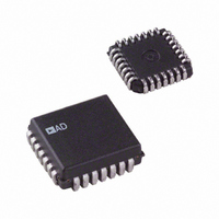
IC DAC 12BIT QUAD READBK 28-PLCC
Manufacturer
Analog Devices Inc
Datasheet
1.DAC8412FPCZ.pdf
(20 pages)
Specifications of DAC8413FPC
Rohs Status
RoHS non-compliant
Settling Time
6µs
Number Of Bits
12
Data Interface
Parallel
Number Of Converters
4
Voltage Supply Source
Single Supply
Power Dissipation (max)
330mW
Operating Temperature
-40°C ~ 85°C
Mounting Type
Surface Mount
Package / Case
28-LCC (J-Lead)
Number Of Channels
4
Resolution
12b
Conversion Rate
167KSPS
Interface Type
Parallel
Single Supply Voltage (typ)
5V
Dual Supply Voltage (typ)
±15V
Architecture
R-2R
Power Supply Requirement
Single/Dual
Output Type
Voltage
Integral Nonlinearity Error
±4LSB
Single Supply Voltage (min)
4.75V
Single Supply Voltage (max)
5.25V
Dual Supply Voltage (min)
±14.25V
Dual Supply Voltage (max)
±15.75V
Operating Temp Range
-40C to 85C
Operating Temperature Classification
Industrial
Mounting
Surface Mount
Pin Count
28
Package Type
PLCC
Lead Free Status / Rohs Status
Not Compliant
Available stocks
Company
Part Number
Manufacturer
Quantity
Price
Company:

Part Number:
DAC8413FPC
Manufacturer:
VISHAY
Quantity:
6 652
Company:
Part Number:
DAC8413FPC
Manufacturer:
Analog Devices Inc
Quantity:
10 000
Part Number:
DAC8413FPC
Manufacturer:
ADI/亚德诺
Quantity:
20 000
Company:
Part Number:
DAC8413FPC-REEL
Manufacturer:
Analog Devices Inc
Quantity:
10 000
Company:
Part Number:
DAC8413FPCZ
Manufacturer:
Analog Devices Inc
Quantity:
10 000
Company:
Part Number:
DAC8413FPCZ-REEL
Manufacturer:
Analog Devices Inc
Quantity:
10 000


DAC8412/DAC8413
THEORY OF OPERATION
INTRODUCTION
The DAC8412/DAC8413 are quad, voltage output, 12-bit parallel
input DACs featuring a 12-bit data bus with readback capability.
The only differences between the DAC8412/DAC8413 are the
reset functions. The DAC8412 resets to midscale (Code 0x800),
and the DAC8413 resets to minimum scale (Code 0x000).
The ability to operate from a single 5 V supply is a unique
feature of these DACs.
Operation of the DAC8412/DAC8413 can be viewed by
dividing the system into three separate functional groups: the
digital I/O and logic, the digital-to-analog converters, and the
output amplifiers.
DACS
Each DAC is a voltage switched, high impedance (R = 50 kΩ),
R-2R ladder configuration. Each 2R resistor is driven by a pair
of switches that connect the resistor to either V
GLITCH
Worst-case glitch occurs at the transition between Half-Scale
Digital Code 1000 0000 0000 to half-scale minus 1 LSB, 0111
1111 1111. It can be measured at about 2 V μs (see Figure 36).
For demanding applications such as waveform generation or
precision instrumentation control, a deglitcher circuit can be
implemented with a standard sample-and-hold circuit (see
Figure 37). When CS is enabled by synchronizing the hold
period to be longer than the glitch tradition, the output voltage
can be smoothed with minimum disturbance. A quad
sample-and-hold amplifier, SMP04, has been used to illustrate
the deglitching result (see
DACOUT
DACOUT
S/H
CS
S/H
1
DACOUT
Figure 37. Data Output (Read Timing)
H
Figure 36
).
S
REFH
H
DACOUT
or V
REFL
1
S
.
Rev. F | Page 14 of 20
REFERENCE INPUTS
All four DACs share common reference high (V
low (V
the output high and low voltage limits of all four of the DACs.
Each reference input has voltage restrictions with respect to the
other reference and to the power supplies. The V
any voltage between V
any value between +V
because of these restrictions, the DAC8412 references cannot be
inverted (that is, V
It is important to note that the DAC8412 V
and sources current. In addition, the input current of both V
and V
current-sinking capability and must be buffered with an
amplifier to drive V
requirements.
It is recommended that the reference inputs be bypassed with
0.2 μF capacitors when operating with ±10 V references. This
limits the reference bandwidth.
DIGITAL I/O
See Table 6 for the digital control logic truth table. Digital I/O
consists of a 12-bit bidirectional data bus, two registers select
inputs, A0 and A1, a R/ W input, a RESET input, a chip select ( CS ),
and a load DAC ( LDAC ) input. Control of the DACs and bus
direction is determined by these inputs as shown in
data bits are labeled with the MSB defined as Data Bit 11 and the
LSB as Data Bit 0. All digital pins are TTL/CMOS compatible.
See Figure 38 for a simplified I/O logic diagram. The register
select inputs A0 and A1 select individual DAC registers A
(Binary Code 00) through D (Binary Code 11). Decoding of the
registers is enabled by the CS input. When CS is high, no
decoding takes place, and neither the writing nor the reading of
the input registers is enabled. The loading of the second bank of
registers is controlled by the asynchronous LDAC input. By
taking LDAC low while CS is enabled, all output registers can
be updated simultaneously. Note that the t
width for updating all DACs is a minimum of 170 ns.
The R/ W input, when enabled by CS , controls the writing to
and reading from the input register.
CODING
Both DAC8412/DAC8413 use binary coding. The output
voltage can be calculated by
where N is the digital code in decimal.
V
REFL
REFL
OUT
) inputs. The voltages applied to these reference inputs set
are code-dependent. Many references have limited
=
V
REFL
+
REFL
REFH
(
SS
V
DD
cannot be greater than V
REFH
and V
. The V
− 2.5 V and V
−
4096
REFH
V
REFL
REFL
− 2.5 V, and V
has no such special
)
×
N
REFL
LDW
+ 2.5 V. Note that
REFH
REFH
required pulse
REFH
input both sinks
REFH
REFL
) and reference
Table 6.
can be set to
).
can be set at
Digital
REFH
Related parts for DAC8413FPC
Image
Part Number
Description
Manufacturer
Datasheet
Request
R

Part Number:
Description:
Analog Standard Cell 8-Bit Digital to Analog Converter
Manufacturer:
AMSCO [austriamicrosystems AG]
Datasheet:

Part Number:
Description:
±1.7g Dual-Axis IMEMS Accelerometer Evaluation Board
Manufacturer:
Analog Devices Inc
Datasheet:

Part Number:
Description:
Inertial Sensor Evaluation System
Manufacturer:
Analog Devices Inc
Datasheet:
Part Number:
Description:
Manufacturer:
Analog Devices Inc
Datasheet:
Part Number:
Description:
Manufacturer:
Analog Devices Inc
Datasheet:
Part Number:
Description:
Manufacturer:
Analog Devices Inc
Datasheet:
Part Number:
Description:
Manufacturer:
Analog Devices Inc
Datasheet:
Part Number:
Description:
Manufacturer:
Analog Devices Inc
Datasheet:
Part Number:
Description:
Manufacturer:
Analog Devices Inc
Datasheet:
Part Number:
Description:
Manufacturer:
Analog Devices Inc
Datasheet:
Part Number:
Description:
Manufacturer:
Analog Devices Inc
Datasheet:
Part Number:
Description:
Manufacturer:
Analog Devices Inc
Datasheet:
Part Number:
Description:
Manufacturer:
Analog Devices Inc
Datasheet: