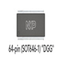
SSTV16859DGG NXP Semiconductors, SSTV16859DGG Datasheet - Page 8

SSTV16859DGG
Manufacturer Part Number
SSTV16859DGG
Description
Manufacturer
NXP Semiconductors
Datasheet
1.SSTV16859DGG.pdf
(14 pages)
Specifications of SSTV16859DGG
Logic Family
SSTV
Logical Function
Registered Buffer
Number Of Elements
1
Number Of Bits
13
Number Of Inputs
13
Number Of Outputs
26
High Level Output Current
-20mA
Low Level Output Current
20mA
Package Type
TSSOP
Propagation Delay Time
2.4ns
Operating Supply Voltage (typ)
2.5V
Operating Supply Voltage (max)
2.7V
Operating Supply Voltage (min)
2.3V
Clock-edge Trigger Type
Posit/Negat-Edge
Polarity
Non-Inverting
Technology
CMOS
Frequency (max)
200(Min)MHz
Mounting
Surface Mount
Pin Count
64
Operating Temp Range
0C to 70C
Operating Temperature Classification
Commercial
Lead Free Status / Rohs Status
Compliant
1. This parameter is not necessarily production tested.
2. Data inputs must be below a minimum time of t
3. Data and clock inputs must be held at valid levels (not floating) a minimum time of t
4. For data signal input slew rate
5. For data signal input slew rate
6. CK, CK signals input slew rates are
Philips Semiconductors
TIMING REQUIREMENTS
Over recommended operating conditions; T
NOTES:
SWITCHING CHARACTERISTICS
Over recommended operating conditions; T
Class I, V
2002 Feb 19
SYMBOL
SYMBOL
2.5 V 13-bit to 26-bit SSTL_2
registered buffer for stacked DDR DIMM
f
t
f
t
clock
inact
t
t
max
PHL
t
t
t
t
act
t
t
SL
pd
su
w
h
REF
= V
Clock frequency
Pulse duration, CK, CK HIGH or LOW
Differential inputs active time
Differential inputs inactive time
Setup time, fast slew rate
(see Notes 4 and 6)
Setup time, slow slew rate
(see Notes 5 and 6)
Hold time, fast slew rate
(see Notes 4 and 6)
Hold time, slow slew rate
(see Notes 5 and 6)
Output slew
CK and CK
RESET
TT
= V
DD
0.5 and C
PARAMETER
(INPUT)
(INPUT)
FROM
1 V/ns.
0.5 V/ns and < 1 V/ns.
O
L
= 10 pF (unless otherwise noted) (see Figure 1)
1 V/ns.
amb
amb
= 0 to +70 C (unless otherwise noted) (see Figure 1)
= 0 to +70 C; V
act
max, after RESET is taken high.
DD
= 2.3 – 2.7 V
Data before CK
Data before CK , CK
TEST CONDITIONS
Data after CK
Data after CK , CK
8
(OUTPUT)
(OUTPUT)
Notes 1, 2
Notes 1, 3
TO
Q
Q
O
.
CK
CK
inact
max, after RESET is taken low.
MIN
MIN
200
2.5
1.1
1.1
V
—
—
—
V
1
DD
DD
= 2.5 V 0.2 V
= 2.5 V 0.2 V
LIMITS
LIMITS
0.75
0.75
0.9
0.9
MAX
MAX
200
SSTV16859
2.8
22
22
—
—
6
5
Product data
UNIT
UNIT
MHz
V/ns
MHz
ns
ns
ns
ns
ns
ns
ns
ns
ns


