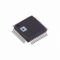
AD9709AST Analog Devices Inc, AD9709AST Datasheet - Page 18

AD9709AST
Manufacturer Part Number
AD9709AST
Description
IC DAC 8BIT DUAL 125MSPS 48-LQFP
Manufacturer
Analog Devices Inc
Series
TxDAC+®r
Datasheet
1.AD9709ASTZRL.pdf
(32 pages)
Specifications of AD9709AST
Rohs Status
RoHS non-compliant
Settling Time
35ns
Number Of Bits
8
Data Interface
Parallel
Number Of Converters
2
Voltage Supply Source
Analog and Digital
Power Dissipation (max)
450mW
Operating Temperature
-40°C ~ 85°C
Mounting Type
Surface Mount
Package / Case
48-LQFP
For Use With
AD9709-EBZ - BOARD EVAL FOR AD9709
Available stocks
Company
Part Number
Manufacturer
Quantity
Price
Company:
Part Number:
AD9709AST
Manufacturer:
ADI
Quantity:
169
Part Number:
AD9709AST
Manufacturer:
ADI/亚德诺
Quantity:
20 000
Company:
Part Number:
AD9709ASTZ
Manufacturer:
ADI
Quantity:
19
Company:
Part Number:
AD9709ASTZ
Manufacturer:
AD
Quantity:
170
Company:
Part Number:
AD9709ASTZ
Manufacturer:
Analog Devices Inc
Quantity:
10 000
Part Number:
AD9709ASTZ
Manufacturer:
ADI/亚德诺
Quantity:
20 000
Company:
Part Number:
AD9709ASTZRL
Manufacturer:
NECTOKIN
Quantity:
4 309
Company:
Part Number:
AD9709ASTZRL
Manufacturer:
Analog Devices Inc
Quantity:
10 000
AD9709
SLEEP MODE OPERATION
The AD9709 has a power-down function that turns off the
output current and reduces the supply current to less than
8.5 mA over the specified supply range of 3.3 V to 5 V and
temperature range. This mode can be activated by applying a
Logic Level 1 to the SLEEP pin. The SLEEP pin logic threshold
is equal to 0.5 × AVDD. This digital input also contains an active
pull-down circuit that ensures the AD9709 remains enabled if
this input is left disconnected. The AD9709 requires less than
50 ns to power down and approximately 5 μs to power back up.
POWER DISSIPATION
The power dissipation, P
factors, including
•
•
•
•
The power dissipation is directly proportional to the analog
supply current, I
is directly proportional to I
insensitive to f
Conversely, I
f
Figure 35 show I
ratios (f
DVDD2 = 5 V and DVDD1 = DVDD2 = 3.3 V, respectively.
Note how I
DVDD1/DVDD2 is reduced from 5 V to 3.3 V.
CLK
, and digital supply (DVDD1/DVDD2). Figure 34 and
the power supply voltages (AVDD and DVDD1/DVDD2)
the full-scale current output (I
the update rate (f
the reconstructed digital input waveform
OUT
/f
DVDD
CLK
DVDD
CLK
) for various update rates with DVDD1 =
is reduced by more than a factor of 2 when
AVDD
DVDD
.
is dependent on the digital input waveform,
, and the digital supply current, I
as a function of full-scale sine wave output
CLK
D
, of the AD9709 is dependent on several
)
OUTFS
, as shown in Figure 33, and is
OUTFS
)
DVDD
. I
AVDD
Rev. B | Page 18 of 32
35
30
25
20
15
10
18
16
14
12
10
80
70
60
50
40
30
20
10
5
0
8
6
4
2
0
0
0
0
Figure 35. I
Figure 34. I
0.1
0.1
5
DVDD
DVDD
Figure 33. I
vs. Ratio @ DVDD1 = DVDD2 = 3.3 V
vs. Ratio @ DVDD1 = DVDD2 = 5 V
RATIO (
RATIO (
0.2
0.2
10
I
OUTFS
125MSPS
100MSPS
65MSPS
25MSPS
AVDD
5MSPS
f
f
OUT
OUT
(mA)
vs. I
/
/
f
f
0.3
CLK
0.3
CLK
15
OUTFS
125MSPS
100MSPS
65MSPS
25MSPS
5MSPS
)
)
0.4
0.4
20
0
0
2
.5
.5
5


