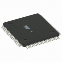
ATF1504BE-7AU100 Atmel, ATF1504BE-7AU100 Datasheet - Page 7

ATF1504BE-7AU100
Manufacturer Part Number
ATF1504BE-7AU100
Description
IC CPLD 64MC 1.8V 100-TQFP
Manufacturer
Atmel
Series
ATF1504BEr
Datasheet
1.ATF1504BE-7AU44.pdf
(30 pages)
Specifications of ATF1504BE-7AU100
Programmable Type
In System Programmable (min 10K program/erase cycles)
Delay Time Tpd(1) Max
7.5ns
Voltage Supply - Internal
1.7 V ~ 1.9 V
Number Of Macrocells
64
Number Of I /o
80
Operating Temperature
-40°C ~ 85°C
Mounting Type
Surface Mount
Package / Case
100-TQFP, 100-VQFP
Features
CMOS/TTL Compatible
Voltage
1.8V
Memory Type
CMOS
For Use With
ATF15XX-DK3 - KIT DEV FOR ATF15XX CPLD'S
Lead Free Status / RoHS Status
Lead free / RoHS Compliant
Number Of Logic Elements/cells
-
Available stocks
Company
Part Number
Manufacturer
Quantity
Price
Company:
Part Number:
ATF1504BE-7AU100
Manufacturer:
TI
Quantity:
1 450
Part Number:
ATF1504BE-7AU100
Manufacturer:
ATMEL/爱特梅尔
Quantity:
20 000
1.3
1.4
1.5
1.6
1.7
3637B–PLD–1/08
Flip-flop
Extra Feedback
I/O Control
Global Bus/Switch Matrix
Foldback Bus
The ATF1504BE’s flip-flop has very flexible data and control functions. The data input can come
from either the XOR gate, from a separate product term or directly from the I/O pin. Selecting the
separate product term allows creation of a buried registered feedback within a combinatorial out-
put macrocell. (This feature is automatically implemented by the fitter software). In addition to D,
T, JK and SR operation, the flip-flop can also be configured as a flow-through latch. In this
mode, data passes through when the clock is high and is latched when the clock is low.
The clock itself can be any one of the Global CLK signals (GCK[0 : 2]) or an individual product
term. The flip-flop changes state on the clock’s rising edge. When the GCK signal is used as the
clock, one of the macrocell product terms can be selected as a clock enable. When the clock
enable function is active and the enable signal (product term) is low, all clock edges are ignored.
The flip-flop’s asynchronous reset signal (AR) can be either the Global Clear (GCLEAR), a prod-
uct term, or always off. AR can also be a logic OR of GCLEAR with a product term. The
asynchronous preset (AP) can be a product term or always off.
The ATF1504BE macrocell output can be selected as registered or combinatorial. The extra bur-
ied feedback signal can be either combinatorial or a registered signal regardless of whether the
output is combinatorial or registered. (This enhancement function is automatically implemented
by the fitter software.) Feedback of a buried combinatorial output allows the creation of a second
latch within a macrocell.
The output enable multiplexer (MOE) controls the output enable signal. Each I/O can be individ-
ually configured as an input, output or bi-directional pin. The output enable for each macrocell
can be selected from the true or complement of the two output enable pins, a subset of the I/O
pins, or a subset of the I/O macrocells. This selection is automatically done by the fitter software
when the I/O is configured as an input or bi-directional pin.
The global bus contains all input and I/O pin signals as well as the buried feedback signal from
all 64 macrocells. The switch matrix in each logic block receives as its inputs all signals from the
global bus. Under software control, up to 40 of these signals can be selected as inputs to the
logic block.
Each macrocell also generates a foldback product term. This signal goes to the regional bus and
is available to all 16 macrocells within the logic block. The foldback is an inverse polarity of one
of the macrocell’s product terms. The 16 foldback terms in each logic block allow generation of
high fan-in sum terms or other complex logic functions with little additional delay.
ATF1504BE
7


