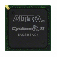
EP2C35F672C7 Altera, EP2C35F672C7 Datasheet - Page 67

EP2C35F672C7
Manufacturer Part Number
EP2C35F672C7
Description
IC CYCLONE II FPGA 33K 672-FBGA
Manufacturer
Altera
Series
Cyclone® IIr
Datasheet
1.EP2C5T144C8N.pdf
(168 pages)
Specifications of EP2C35F672C7
Number Of Logic Elements/cells
33216
Number Of Labs/clbs
2076
Total Ram Bits
483840
Number Of I /o
475
Voltage - Supply
1.15 V ~ 1.25 V
Mounting Type
Surface Mount
Operating Temperature
0°C ~ 85°C
Package / Case
672-FBGA
For Use With
P0301 - DE2 CALL FOR ACADEMIC PRICING544-1733 - PCI KIT W/CYCLONE II EP2C35N
Lead Free Status / RoHS Status
Contains lead / RoHS non-compliant
Number Of Gates
-
Other names
544-1088
EP2C35F672C7ES
EP2C35F672C7ES
Available stocks
Company
Part Number
Manufacturer
Quantity
Price
Company:
Part Number:
EP2C35F672C7N
Manufacturer:
ALTERA
Quantity:
170
Part Number:
EP2C35F672C7N
Manufacturer:
ALTERA/阿尔特拉
Quantity:
20 000
Altera Corporation
February 2007
f
You can use I/O pins and internal logic to implement a high-speed I/O
receiver and transmitter in Cyclone II devices. Cyclone II devices do not
contain dedicated serialization or deserialization circuitry. Therefore,
shift registers, internal PLLs, and IOEs are used to perform
serial-to-parallel conversions on incoming data and parallel-to-serial
conversion on outgoing data.
The maximum internal clock frequency for a receiver and for a
transmitter is 402.5 MHz. The maximum input data rate of 805 Mbps and
the maximum output data rate of 640 Mbps is only achieved when DDIO
registers are used. The LVDS standard does not require an input
reference voltage, but it does require a 100-Ω termination resistor
between the two signals at the input buffer. An external resistor network
is required on the transmitter side.
For more information on Cyclone II differential I/O interfaces, see the
High-Speed Differential Interfaces in Cyclone II Devices chapter in Volume 1
of the Cyclone II Device Handbook.
Series On-Chip Termination
On-chip termination helps to prevent reflections and maintain signal
integrity. This also minimizes the need for external resistors in high pin
count ball grid array (BGA) packages. Cyclone II devices provide I/O
driver on-chip impedance matching and on-chip series termination for
single-ended outputs and bidirectional pins.
Note to
(1)
EP2C70
Table 2–18. Cyclone II Device LVDS Channels (Part 2 of 2)
The first number represents the number of bidirectional I/O pins which can be
used as inputs or outputs. The number in parenthesis includes dedicated clock
input pin pairs which can only be used as inputs.
Table
Device
2–18:
Pin Count
672
896
Cyclone II Device Handbook, Volume 1
Cyclone II Architecture
Number of LVDS
Channels
160 (168)
257 (265)
(1)
2–55


