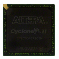
EP2C35F672C6N Altera, EP2C35F672C6N Datasheet - Page 97

EP2C35F672C6N
Manufacturer Part Number
EP2C35F672C6N
Description
IC CYCLONE II FPGA 33K 672-FBGA
Manufacturer
Altera
Series
Cyclone® IIr
Datasheet
1.EP2C5T144C8N.pdf
(168 pages)
Specifications of EP2C35F672C6N
Number Of Logic Elements/cells
33216
Number Of Labs/clbs
2076
Total Ram Bits
483840
Number Of I /o
475
Voltage - Supply
1.15 V ~ 1.25 V
Mounting Type
Surface Mount
Operating Temperature
0°C ~ 85°C
Package / Case
672-FBGA
Family Name
Cyclone® II
Number Of Logic Blocks/elements
33216
# I/os (max)
475
Frequency (max)
500MHz
Process Technology
90nm
Operating Supply Voltage (typ)
1.2V
Logic Cells
33216
Ram Bits
483840
Operating Supply Voltage (min)
1.15V
Operating Supply Voltage (max)
1.25V
Operating Temp Range
0C to 85C
Operating Temperature Classification
Commercial
Mounting
Surface Mount
Pin Count
672
Package Type
FBGA
For Use With
P0301 - DE2 CALL FOR ACADEMIC PRICING544-1733 - PCI KIT W/CYCLONE II EP2C35N649-1001 - KIT DEV CYCLONE II PCI EXPRESS
Lead Free Status / RoHS Status
Lead free / RoHS Compliant
Number Of Gates
-
Lead Free Status / Rohs Status
Compliant
Other names
544-1694
Available stocks
Company
Part Number
Manufacturer
Quantity
Price
Company:
Part Number:
EP2C35F672C6N
Manufacturer:
ALTERA
Quantity:
170
Altera Corporation
February 2008
Notes to
(1)
(2)
1.5-V HSTL class I
1.5V HSTL class II
Table 5–7. DC Characteristics of User I/O Pins Using Single-Ended Standards
I/O Standard
The values in this table are based on the conditions listed in
This specification is supported across all the programmable drive settings available as shown in the
Architecture
Table
5–7:
chapter of the Cyclone II Device Handbook.
I
OL
16
(mA)
Differential I/O Standards
The RSDS and mini-LVDS I/O standards are only supported on output
pins. The LVDS I/O standard is supported on both receiver input pins
and transmitter output pins.
1
Figure 5–1
standards (LVDS, LVPECL, differential 1.5-V HSTL class I and II,
differential 1.8-V HSTL class I and II, differential SSTL-2 class I and II, and
differential SSTL-18 class I and II).
8
Test Conditions
For more information on how these differential I/O standards
are implemented, refer to the
Cyclone II Devices
shows the receiver input waveforms for all differential I/O
I
OH
–16
–8
(mA)
chapter of the Cyclone II Device Handbook.
Tables 5–2
Maximum V
DC Characteristics and Timing Specifications
0.4
0.4
Cyclone II Device Handbook, Volume 1
and 5–6.
High-Speed Differential Interfaces in
Voltage Thresholds
OL
(V)
Notes
(1),
Minimum V
V
V
(2)
C C I O
C C I O
(Part 2 of 2)
Cyclone II
– 0.4
– 0.4
OH
(V)
5–7


