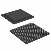
XC3S1200E-4FGG400C Xilinx Inc, XC3S1200E-4FGG400C Datasheet - Page 177

XC3S1200E-4FGG400C
Manufacturer Part Number
XC3S1200E-4FGG400C
Description
IC SPARTAN-3E FPGA 1200K 400FBGA
Manufacturer
Xilinx Inc
Series
Spartan™-3Er
Datasheet
1.XC3S100E-4VQG100C.pdf
(233 pages)
Specifications of XC3S1200E-4FGG400C
Total Ram Bits
516096
Number Of Logic Elements/cells
19512
Number Of Labs/clbs
2168
Number Of I /o
304
Number Of Gates
1200000
Voltage - Supply
1.14 V ~ 1.26 V
Mounting Type
Surface Mount
Operating Temperature
0°C ~ 85°C
Package / Case
400-BGA
No. Of Logic Blocks
19512
No. Of Gates
1200000
No. Of Macrocells
19512
No. Of Speed Grades
4
No. Of I/o's
304
Clock Management
DLL
Lead Free Status / RoHS Status
Lead free / RoHS Compliant
Other names
122-1480
Available stocks
Company
Part Number
Manufacturer
Quantity
Price
Company:
Part Number:
XC3S1200E-4FGG400C
Manufacturer:
XILINX
Quantity:
184
Company:
Part Number:
XC3S1200E-4FGG400C
Manufacturer:
Xilinx Inc
Quantity:
10 000
Part Number:
XC3S1200E-4FGG400C
Manufacturer:
XILINX/赛灵思
Quantity:
20 000
User I/Os by Bank
Table 134
tributed on the XC3S100E FPGA packaged in the CP132
package.
Table 134: User I/Os Per Bank for the XC3S100E in the CP132 Package
Table 135: User I/Os Per Bank for the XC3S250E and XC3S500E in the CP132 Package
DS312-4 (v3.8) August 26, 2009
Product Specification
Notes:
1.
2.
Notes:
1.
2.
Top
Right
Bottom
Left
TOTAL
Top
Right
Bottom
Left
TOTAL
Package
Package
Some VREF and CLK pins are on INPUT pins.
The eight global clock pins in this bank have optional functionality during configuration and are counted in the DUAL column.
Some VREF and CLK pins are on INPUT pins.
The eight global clock pins in this bank have optional functionality during configuration and are counted in the DUAL column.
Edge
Edge
Table 135
shows how the 83 available user-I/O pins are dis-
R
I/O Bank
I/O Bank
indicates how the 92 available user-I/O
0
1
2
3
0
1
2
3
Maximum
Maximum
I/O
I/O
18
23
22
20
83
22
23
26
21
92
I/O
I/O
10
16
11
11
22
6
0
0
0
0
www.xilinx.com
pins are distributed on the XC3S250E and the XC3S500E
FPGAs in the CP132 package.
INPUT
INPUT
2
0
0
0
2
0
0
0
0
0
All Possible I/O Pins by Type
All Possible I/O Pins by Type
DUAL
DUAL
21
20
42
21
24
46
1
0
1
0
VREF
VREF
1
2
2
2
7
2
2
2
2
8
Pinout Descriptions
(1)
(1)
CLK
CLK
0
0
0
0
16
16
8
8
8
8
(2)
(2)
(2)
(2)
(1)
(1)
177


