XC4VLX25-10SFG363C Xilinx Inc, XC4VLX25-10SFG363C Datasheet - Page 14
XC4VLX25-10SFG363C
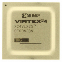
Manufacturer Part Number
XC4VLX25-10SFG363C
Description
IC FPGA VIRTEX-4 24K 363-FCBGA
Manufacturer
Xilinx Inc
Series
Virtex™-4r
Specifications of XC4VLX25-10SFG363C
Number Of Logic Elements/cells
24192
Number Of Labs/clbs
2688
Total Ram Bits
1327104
Number Of I /o
240
Voltage - Supply
1.14 V ~ 1.26 V
Mounting Type
Surface Mount
Operating Temperature
0°C ~ 85°C
Package / Case
363-FBGA, FCBGA
For Use With
807-1004 - DAUGHTER CARD WITH VIRTEX-4122-1523 - EVALUATION PLATFORM VIRTEX-4
Lead Free Status / RoHS Status
Lead free / RoHS Compliant
Number Of Gates
-
Other names
122-1489
Available stocks
Company
Part Number
Manufacturer
Quantity
Price
Company:

Part Number:
XC4VLX25-10SFG363C
Manufacturer:
XILINX
Quantity:
689
Company:
Part Number:
XC4VLX25-10SFG363C
Manufacturer:
Xilinx Inc
Quantity:
10 000


Table 16: Processor Block Switching Characteristics
Table 17: Processor Block PLB Switching Characteristics
Table 18: Processor Block JTAG Switching Characteristics
DS302 (v3.7) September 9, 2009
Product Specification
Setup and Hold Relative to Clock (CPMC405CLOCK)
Clock to Out
Clock
Setup and Hold Relative to Clock (PLBCLK)
Clock to Out
Setup and Hold Relative to Clock (JTAGC405TCK)
Clock to Out
Clock and Power Management control inputs
Reset control inputs
Debug control inputs
Trace control inputs
External Interrupt Controller control inputs
Clock and Power Management control outputs
Reset control outputs
Debug control outputs
Trace control outputs
CPMC405CLOCK minimum pulse width, High
CPMC405CLOCK minimum pulse width, Low
Processor Local Bus (ICU/DCU) control inputs
Processor Local Bus (ICU/DCU) data inputs
Processor Local Bus (ICU/DCU) control outputs
Processor Local Bus (ICU/DCU) address bus outputs
Processor Local Bus (ICU/DCU) data bus outputs
JTAG control inputs
JTAG reset input
JTAG control outputs
Description
Description
Description
T
T
T
T
T
PPCDCK
PPCCKD
PPCDCK
PPCCKD
PPCCKO
T
T
T
T
T
T
T
T
T
T
T
T
T
T
T
T
PPCDCK
PPCCKD
PPCDCK
PPCCKD
PPCDCK
PPCCKD
PPCDCK
PPCCKD
PPCDCK
PPCCKD
PPCCKO
PPCCKO
PPCCKO
PPCCKO
CPWH
CPWL
_JTGTDI
_JTGTDI
_JTGTRSTN
_JTGTRSTN
_JTGTDO
Symbol
www.xilinx.com
T
T
T
T
T
T
T
Symbol
_CORECKI/
_CORECKI
_RSTCHIP/
_RSTCHIP
_EXBUSHAK/
_EXBUSHAK
_TRCDIS/
_TRCDIS
_CINPIRQ/
_CINPIRQ
_CORESLP
_RSTCHIP
_DBGLDAPU
_TRCCYCLE
PPCCKO
PPCDCK
PPCCKD
PPCDCK
PPCCKD
PPCCKO
PPCCKO
Virtex-4 FPGA Data Sheet: DC and Switching Characteristics
Symbol
_DCUWRDBUS
_ICUBUSY/
_ICUBUSY
_ICURDDB/
_ICURDDB
_DCUABORT
_ICUABUS
0.60
0.20
0.60
0.20
0.60
0.20
0.60
0.20
1.04
0.20
1.35
1.44
1.34
1.52
1.11
1.11
1.68
-12
1.16
0.20
0.60
0.20
-12
0.60
0.20
0.90
0.20
1.61
1.66
2.08
-12
Speed Grade
Speed Grade
Speed Grade
0.65
0.20
0.65
0.20
0.65
0.20
0.65
0.20
1.15
0.20
1.59
1.48
1.68
1.25
1.25
1.51
1.79
1.29
0.20
0.65
0.20
-11
-11
0.66
0.20
1.00
0.20
1.78
1.85
2.24
-11
0.74
0.23
0.74
0.23
0.74
0.23
0.74
0.23
1.40
0.23
1.74
1.83
1.70
1.83
1.43
1.43
1.48
0.23
0.74
0.23
2.14
-10
-10
0.76
0.23
1.15
0.23
2.05
2.13
2.57
-10
ns, Max
ns, Max
ns, Max
ns, Max
ns, Max
ns, Max
ns, Max
ns, Max
ns, Min
ns, Min
ns, Min
ns, Min
ns, Min
ns, Min
ns, Min
ns, Min
ns, Min
ns, Min
ns, Min
Units
Units
Units
14
Related parts for XC4VLX25-10SFG363C
Image
Part Number
Description
Manufacturer
Datasheet
Request
R

Part Number:
Description:
IC FPGA VIRTEX-4 24K 668-FCBGA
Manufacturer:
Xilinx Inc
Datasheet:

Part Number:
Description:
IC FPGA VIRTEX-4 LX 25K 363FCBGA
Manufacturer:
Xilinx Inc
Datasheet:

Part Number:
Description:
IC FPGA VIRTEX-4 LX 25K 363FCBGA
Manufacturer:
Xilinx Inc
Datasheet:

Part Number:
Description:
IC FPGA VIRTEX-4 24K 668-FCBGA
Manufacturer:
Xilinx Inc
Datasheet:
Part Number:
Description:
IC FPGA VIRTEX-4 LX 25K 668FCBGA
Manufacturer:
Xilinx Inc
Datasheet:
Part Number:
Description:
IC FPGA VIRTEX-4 LX 25K 363FCBGA
Manufacturer:
Xilinx Inc
Datasheet:
Part Number:
Description:
IC FPGA VIRTEX-4 LX 25K 363FCBGA
Manufacturer:
Xilinx Inc
Datasheet:

Part Number:
Description:
IC FPGA VIRTEX-4 LX 25K 676-FBGA
Manufacturer:
Xilinx Inc
Datasheet:
Part Number:
Description:
IC FPGA VIRTEX-4 LX 25K 676-FBGA
Manufacturer:
Xilinx Inc
Datasheet:
Part Number:
Description:
IC FPGA VIRTEX-4 LX 25K 668FCBGA
Manufacturer:
Xilinx Inc
Datasheet:
Part Number:
Description:
IC FPGA VIRTEX-4 LX 25K 668FCBGA
Manufacturer:
Xilinx Inc
Datasheet:
Part Number:
Description:
IC FPGA VIRTEX-4 LX 25K 676-FBGA
Manufacturer:
Xilinx Inc
Datasheet:
Part Number:
Description:
IC FPGA VIRTEX-4 LX 25K 676-FBGA
Manufacturer:
Xilinx Inc
Datasheet:
Part Number:
Description:
IC FPGA VIRTEX-4LX 363FCBGA
Manufacturer:
Xilinx Inc
Datasheet:
Part Number:
Description:
IC FPGA VIRTEX-4LX 363FCBGA
Manufacturer:
Xilinx Inc
Datasheet: