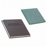
EP2S30F672I4 Altera, EP2S30F672I4 Datasheet - Page 138

EP2S30F672I4
Manufacturer Part Number
EP2S30F672I4
Description
IC STRATIX II FPGA 30K 672-FBGA
Manufacturer
Altera
Series
Stratix® IIr
Datasheet
1.EP2S15F484I4N.pdf
(238 pages)
Specifications of EP2S30F672I4
Number Of Logic Elements/cells
33880
Number Of Labs/clbs
1694
Total Ram Bits
1369728
Number Of I /o
500
Voltage - Supply
1.15 V ~ 1.25 V
Mounting Type
Surface Mount
Operating Temperature
-40°C ~ 100°C
Package / Case
672-FBGA
Family Name
Stratix II
Number Of Logic Blocks/elements
33880
# I/os (max)
500
Frequency (max)
711.24MHz
Process Technology
90nm (CMOS)
Operating Supply Voltage (typ)
1.2V
Logic Cells
33880
Ram Bits
1369728
Operating Supply Voltage (min)
1.15V
Operating Supply Voltage (max)
1.25V
Operating Temp Range
-40C to 100C
Operating Temperature Classification
Industrial
Mounting
Surface Mount
Pin Count
672
Package Type
FC-FBGA
Lead Free Status / RoHS Status
Contains lead / RoHS non-compliant
Number Of Gates
-
Lead Free Status / Rohs Status
Not Compliant
Other names
544-1899
EP2S30F672I4
EP2S30F672I4
Available stocks
Company
Part Number
Manufacturer
Quantity
Price
Company:
Part Number:
EP2S30F672I4
Manufacturer:
ALTERA
Quantity:
3 000
Company:
Part Number:
EP2S30F672I4N
Manufacturer:
ALTERA
Quantity:
238
Operating Conditions
5–2
Stratix II Device Handbook, Volume 1
V
V
V
V
V
V
V
Symbol
Table 5–3. Stratix II Device Recommended Operating Conditions (Part 1 of 2)
CCINT
CCIO
CCPD
CCA
CCD
I
O
Supply voltage for internal logic
Supply voltage for input and
output buffers, 3.3-V operation
Supply voltage for input and
output buffers, 2.5-V operation
Supply voltage for input and
output buffers, 1.8-V operation
Supply voltage for output buffers,
1.5-V operation
Supply voltage for input and
output buffers, 1.2-V operation
Supply voltage for pre-drivers as
well as configuration and JTAG
I/O buffers.
Analog power supply for PLLs
Digital power supply for PLLs
Input voltage (see
Output voltage
Parameter
Table
Recommended Operating Conditions
Table 5–3
conditions.
Table 5–2. Maximum Duty Cycles in Voltage Transitions
Symbol
5–2)
V
I
contains the Stratix II device family recommended operating
Maximum duty cycles
in voltage transitions
100 μs ≤ risetime ≤ 100 ms
100 μs ≤ risetime ≤ 100 ms (3),
100 μs ≤ risetime ≤ 100 ms
100 μs ≤ risetime ≤ 100 ms
100 μs ≤ risetime ≤ 100 ms
100 μs ≤ risetime ≤ 100 ms
100 μs ≤ risetime ≤ 100 ms
100 μs ≤ risetime ≤ 100 ms
100 μs ≤ risetime ≤ 100 ms
(2),
(5)
Parameter
Conditions
Condition
V
V
V
V
V
V
I
I
I
I
I
I
(3)
(3)
(3)
(3)
(3)
(3)
(3)
(4)
= 4.0 V
= 4.1 V
= 4.2 V
= 4.3 V
= 4.4 V
= 4.5 V
(6)
Minimum
(3.00)
3.135
2.375
1.425
3.135
1.15
1.71
1.14
1.15
1.15
–0.5
0
Note (1)
Duty Cycles
Maximum
100
Altera Corporation
90
50
30
17
10
Maximum Unit
(3.60)
3.465
2.625
1.575
3.465
V
1.25
1.89
1.26
1.25
1.25
4.0
CCIO
April 2011
Unit
%
%
%
%
%
%
V
V
V
V
V
V
V
V
V
V
V


