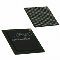
EP2C70F896C7 Altera, EP2C70F896C7 Datasheet - Page 61

EP2C70F896C7
Manufacturer Part Number
EP2C70F896C7
Description
IC CYCLONE II FPGA 70K 896-FBGA
Manufacturer
Altera
Series
Cyclone® IIr
Datasheet
1.EP2C5T144C8N.pdf
(168 pages)
Specifications of EP2C70F896C7
Number Of Logic Elements/cells
68416
Number Of Labs/clbs
4276
Total Ram Bits
1152000
Number Of I /o
622
Voltage - Supply
1.15 V ~ 1.25 V
Mounting Type
Surface Mount
Operating Temperature
0°C ~ 85°C
Package / Case
896-FBGA
For Use With
P0304 - DE2-70 CALL FOR ACADEMIC PRICING544-1703 - VIDEO KIT W/CYCLONE II EP2C70N544-1699 - DSP KIT W/CYCLONE II EPS2C70N
Lead Free Status / RoHS Status
Contains lead / RoHS non-compliant
Number Of Gates
-
Other names
544-1452
Available stocks
Company
Part Number
Manufacturer
Quantity
Price
Part Number:
EP2C70F896C7
Manufacturer:
ALTERA/阿尔特拉
Quantity:
20 000
Company:
Part Number:
EP2C70F896C7N
Manufacturer:
ALTERA
Quantity:
3
Altera Corporation
February 2007
Programmable Drive Strength
The output buffer for each Cyclone II device I/O pin has a programmable
drive strength control for certain I/O standards. The LVTTL, LVCMOS,
SSTL-2 class I and II, SSTL-18 class I and II, HSTL-18 class I and II, and
HSTL-1.5 class I and II standards have several levels of drive strength that
you can control. Using minimum settings provides signal slew rate
control to reduce system noise and signal overshoot.
the possible settings for the I/O standards with drive strength control.
LVTTL (3.3 V)
LVCMOS (3.3 V)
LVTTL/LVCMOS (2.5 V)
LVTTL/LVCMOS (1.8 V)
Table 2–16. Programmable Drive Strength (Part 1 of 2)
I/O Standard
Top & Bottom I/O Pins
I
OH
/I
12
16
20
24
12
16
20
24
12
16
10
12
OL
Cyclone II Device Handbook, Volume 1
4
8
4
8
4
8
2
4
6
8
Current Strength Setting (mA)
Cyclone II Architecture
Table 2–16
Side I/O Pins
Note (1)
12
16
20
24
12
10
12
4
8
4
8
4
8
2
4
6
8
shows
2–49


