EP1SGX25DF672C5N Altera, EP1SGX25DF672C5N Datasheet - Page 92
EP1SGX25DF672C5N
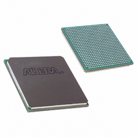
Manufacturer Part Number
EP1SGX25DF672C5N
Description
IC STRATIX GX FPGA 25K 672-FBGA
Manufacturer
Altera
Series
Stratix® GXr
Datasheet
1.EP1SGX10CF672C7N.pdf
(272 pages)
Specifications of EP1SGX25DF672C5N
Number Of Logic Elements/cells
25660
Number Of Labs/clbs
2566
Total Ram Bits
1944576
Number Of I /o
455
Voltage - Supply
1.425 V ~ 1.575 V
Mounting Type
Surface Mount
Operating Temperature
0°C ~ 85°C
Package / Case
672-FBGA
Lead Free Status / RoHS Status
Lead free / RoHS Compliant
Number Of Gates
-
Available stocks
Company
Part Number
Manufacturer
Quantity
Price
Company:

Part Number:
EP1SGX25DF672C5N
Manufacturer:
ALTERA
Quantity:
3 000


TriMatrix Memory
Figure 4–15. M512 RAM Block LAB Row Interface
4–26
Stratix GX Device Handbook, Volume 1
Direct link
interconnect
to adjacent LAB
Direct link
interconnect
from adjacent LAB
C4 and C8
Interconnects
8
Small RAM Block Local
Interconnect Region
10
M4K RAM Blocks
The M4K RAM block includes support for true dual-port RAM. The M4K
RAM block implements buffers for a wide variety of applications such as
storing processor code, implementing lookup schemes, and
implementing larger memory applications. Each block contains
4,608 RAM bits (including parity bits). M4K RAM blocks can be
configured in the following modes:
■
■
■
■
■
■
When configured as RAM or ROM, you can use an initialization file to
pre-load the memory contents.
True dual-port RAM
Simple dual-port RAM
Single-port RAM
FIFO
ROM
Shift register
2
datain
Clocks
M512 RAM
LAB Row Clocks
Block
dataout
address
Signals
Control
Altera Corporation
Direct link
interconnect
to adjacent LAB
Direct link
interconnect
from adjacent LAB
R4 and R8
Interconnects
February 2005
Related parts for EP1SGX25DF672C5N
Image
Part Number
Description
Manufacturer
Datasheet
Request
R

Part Number:
Description:
Stratix Gx Device Family Data Sheet
Manufacturer:
Altera Corporation
Datasheet:

Part Number:
Description:
CYCLONE II STARTER KIT EP2C20N
Manufacturer:
Altera
Datasheet:

Part Number:
Description:
CPLD, EP610 Family, ECMOS Process, 300 Gates, 16 Macro Cells, 16 Reg., 16 User I/Os, 5V Supply, 35 Speed Grade, 24DIP
Manufacturer:
Altera Corporation
Datasheet:
Part Number:
Description:
CPLD, EP610 Family, ECMOS Process, 300 Gates, 16 Macro Cells, 16 Reg., 16 User I/Os, 5V Supply, 15 Speed Grade, 24DIP
Manufacturer:
Altera Corporation
Datasheet:
Part Number:
Description:
Manufacturer:
Altera Corporation
Datasheet:
Part Number:
Description:
CPLD, EP610 Family, ECMOS Process, 300 Gates, 16 Macro Cells, 16 Reg., 16 User I/Os, 5V Supply, 30 Speed Grade, 24DIP
Manufacturer:
Altera Corporation
Datasheet:
Part Number:
Description:
High-performance, low-power erasable programmable logic devices with 8 macrocells, 10ns
Manufacturer:
Altera Corporation
Datasheet:
Part Number:
Description:
High-performance, low-power erasable programmable logic devices with 8 macrocells, 7ns
Manufacturer:
Altera Corporation
Datasheet:
Part Number:
Description:
Classic EPLD
Manufacturer:
Altera Corporation
Datasheet:
Part Number:
Description:
High-performance, low-power erasable programmable logic devices with 8 macrocells, 10ns
Manufacturer:
Altera Corporation
Datasheet:
Part Number:
Description:
Manufacturer:
Altera Corporation
Datasheet:
Part Number:
Description:
Manufacturer:
Altera Corporation
Datasheet:
Part Number:
Description:
Manufacturer:
Altera Corporation
Datasheet: