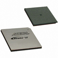
EP2S130F1508C4 Altera, EP2S130F1508C4 Datasheet - Page 62

EP2S130F1508C4
Manufacturer Part Number
EP2S130F1508C4
Description
IC STRATIX II FPGA 130K 1508-FBG
Manufacturer
Altera
Series
Stratix® IIr
Datasheet
1.EP2S15F484I4N.pdf
(238 pages)
Specifications of EP2S130F1508C4
Number Of Logic Elements/cells
132540
Number Of Labs/clbs
6627
Total Ram Bits
6747840
Number Of I /o
1126
Voltage - Supply
1.15 V ~ 1.25 V
Mounting Type
Surface Mount
Operating Temperature
0°C ~ 85°C
Package / Case
1508-FBGA
Lead Free Status / RoHS Status
Contains lead / RoHS non-compliant
Number Of Gates
-
Other names
544-1460
Available stocks
Company
Part Number
Manufacturer
Quantity
Price
Part Number:
EP2S130F1508C4ES
Manufacturer:
ALTERA/阿尔特拉
Quantity:
20 000
Company:
Part Number:
EP2S130F1508C4N
Manufacturer:
ALTERA
Quantity:
490
Part Number:
EP2S130F1508C4N
Manufacturer:
ALTERA/阿尔特拉
Quantity:
20 000
PLLs & Clock Networks
2–54
Stratix II Device Handbook, Volume 1
1
Figures 2–37
clock, regional clock, and PLL external clock output, respectively.
Figure 2–37. Global Clock Control Blocks
Notes to
(1)
(2)
These clock select signals can be dynamically controlled through internal logic
when the device is operating in user mode.
These clock select signals can only be set through a configuration file (.sof or .pof)
and cannot be dynamically controlled during user mode operation.
Figure
CLKSELECT[1..0]
When using the global or regional clock control blocks in
Stratix II devices to select between multiple clocks or to enable
and disable clock networks, be aware of possible narrow pulses
or glitches when switching from one clock signal to another. A
glitch or runt pulse has a width that is less than the width of the
highest frequency input clock signal. To prevent logic errors
within the FPGA, Altera recommends that you build circuits
that filter out glitches and runt pulses.
(1)
This multiplexer supports
User-Controllable
Dynamic Switching
through
PLL Counter
2–37:
Outputs
2–39
2
2
show the clock control block for the global
CLKp
Pins
2
Enable/
Disable
GCLK
CLKn
Pin
Internal
Logic
Internal
Static Clock Select
Logic
Altera Corporation
(2)
May 2007


