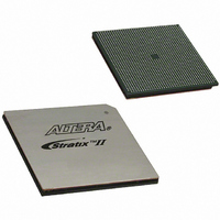
EP2SGX130GF1508I4 Altera, EP2SGX130GF1508I4 Datasheet - Page 219

EP2SGX130GF1508I4
Manufacturer Part Number
EP2SGX130GF1508I4
Description
IC STRATIX II GX 130K 1508-FBGA
Manufacturer
Altera
Series
Stratix® II GXr
Datasheet
1.EP2SGX30DF780C5.pdf
(316 pages)
Specifications of EP2SGX130GF1508I4
Number Of Logic Elements/cells
132540
Number Of Labs/clbs
6627
Total Ram Bits
6747840
Number Of I /o
734
Voltage - Supply
1.15 V ~ 1.25 V
Mounting Type
Surface Mount
Operating Temperature
-40°C ~ 100°C
Package / Case
1508-FBGA
Family Name
Stratix II GX
Number Of Logic Blocks/elements
132540
# I/os (max)
734
Frequency (max)
732.1MHz
Process Technology
SRAM
Operating Supply Voltage (typ)
1.2V
Logic Cells
132540
Ram Bits
6747840
Operating Supply Voltage (min)
1.15V
Operating Supply Voltage (max)
1.25V
Operating Temp Range
-40C to 100C
Operating Temperature Classification
Industrial
Mounting
Surface Mount
Pin Count
1508
Package Type
FC-FBGA
Lead Free Status / RoHS Status
Contains lead / RoHS non-compliant
Number Of Gates
-
Lead Free Status / Rohs Status
Not Compliant
Other names
544-2174
Available stocks
Company
Part Number
Manufacturer
Quantity
Price
Company:
Part Number:
EP2SGX130GF1508I4N
Manufacturer:
Sunon
Quantity:
1 000
Part Number:
EP2SGX130GF1508I4N
Manufacturer:
ALTERA/阿尔特拉
Quantity:
20 000
- Current page: 219 of 316
- Download datasheet (2Mb)
Altera Corporation
June 2009
Note to
(1)
V
V
V
V
V
R
V
V
V
V
V
V
V
V
V
V
V
Table 4–32. LVPECL Specifications
Table 4–33. 3.3-V PCI Specifications
Table 4–34. PCI-X Mode 1 Specifications
Symbol
Symbol
Symbol
CCIO
ID
ICM
OD
OCM
CCIO
IH
IL
OH
OL
CCIO
IH
IL
IPU
OH
OL
L
The top and bottom clock input differential buffers in I/O banks 3, 4, 7, and 8 are powered by V
The PLL clock output/feedback differential buffers are powered by VCC_PLL_OUT. For differential clock
output/feedback operation, connect VCC_PLL_OUT to 3.3 V.
(1)
Table
I/O supply voltage
Input differential voltage
swing (single-ended)
Input common mode voltage
Output differential voltage
(single-ended)
Output common mode
voltage
Receiver differential input
resistor
Output supply voltage
High-level input voltage
Low-level input voltage
High-level output voltage
Low-level output voltage
Output supply voltage
High-level input voltage
Low-level input voltage
Input pull-up voltage
High-level output voltage
Low-level output voltage
4–32:
Parameter
Parameter
Parameter
R
R
L
L
I
I
I
I
OUT
OUT
OUT
OUT
= 100 Ω
= 100 Ω
Conditions
Conditions
Conditions
= –500 μA
= 1,500 μA
= –500 μA
= 1,500 μA
Minimum
Minimum
Minimum
0.5 V
0.9 V
0.5 V
0.7 V
0.9 V
3.135
1,650
–0.3
–0.3
300
525
3.0
3.0
1.0
Stratix II GX Device Handbook, Volume 1
90
CCIO
CCIO
CCIO
CCIO
CCIO
DC and Switching Characteristics
Typical
Typical
Typical
600
100
3.3
3.3
V
V
0.35 V
Maximum
Maximum
Maximum
0.3 V
0.1 V
0.1 V
CCIO
CCIO
CCINT
3.465
1,000
2,250
970
110
3.6
3.6
2.5
+ 0.5
+ 0.5
CCIO
CCIO
CCIO
, not V
CCIO
CCIO
Unit
Unit
Unit
4–49
mV
mV
mV
V
V
V
V
V
V
V
V
V
V
V
V
V
Ω
.
Related parts for EP2SGX130GF1508I4
Image
Part Number
Description
Manufacturer
Datasheet
Request
R

Part Number:
Description:
CYCLONE II STARTER KIT EP2C20N
Manufacturer:
Altera
Datasheet:

Part Number:
Description:
CPLD, EP610 Family, ECMOS Process, 300 Gates, 16 Macro Cells, 16 Reg., 16 User I/Os, 5V Supply, 35 Speed Grade, 24DIP
Manufacturer:
Altera Corporation
Datasheet:

Part Number:
Description:
CPLD, EP610 Family, ECMOS Process, 300 Gates, 16 Macro Cells, 16 Reg., 16 User I/Os, 5V Supply, 15 Speed Grade, 24DIP
Manufacturer:
Altera Corporation
Datasheet:

Part Number:
Description:
Manufacturer:
Altera Corporation
Datasheet:

Part Number:
Description:
CPLD, EP610 Family, ECMOS Process, 300 Gates, 16 Macro Cells, 16 Reg., 16 User I/Os, 5V Supply, 30 Speed Grade, 24DIP
Manufacturer:
Altera Corporation
Datasheet:

Part Number:
Description:
High-performance, low-power erasable programmable logic devices with 8 macrocells, 10ns
Manufacturer:
Altera Corporation
Datasheet:

Part Number:
Description:
High-performance, low-power erasable programmable logic devices with 8 macrocells, 7ns
Manufacturer:
Altera Corporation
Datasheet:

Part Number:
Description:
Classic EPLD
Manufacturer:
Altera Corporation
Datasheet:

Part Number:
Description:
High-performance, low-power erasable programmable logic devices with 8 macrocells, 10ns
Manufacturer:
Altera Corporation
Datasheet:

Part Number:
Description:
Manufacturer:
Altera Corporation
Datasheet:

Part Number:
Description:
Manufacturer:
Altera Corporation
Datasheet:

Part Number:
Description:
Manufacturer:
Altera Corporation
Datasheet:

Part Number:
Description:
CPLD, EP610 Family, ECMOS Process, 300 Gates, 16 Macro Cells, 16 Reg., 16 User I/Os, 5V Supply, 25 Speed Grade, 24DIP
Manufacturer:
Altera Corporation
Datasheet:


