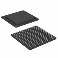
XC3S1600E-4FGG400I Xilinx Inc, XC3S1600E-4FGG400I Datasheet - Page 129

XC3S1600E-4FGG400I
Manufacturer Part Number
XC3S1600E-4FGG400I
Description
IC FPGA SPARTAN-3E 1600K 400FBGA
Manufacturer
Xilinx Inc
Series
Spartan™-3Er
Datasheet
1.XC3S100E-4VQG100C.pdf
(233 pages)
Specifications of XC3S1600E-4FGG400I
Number Of Logic Elements/cells
33192
Number Of Labs/clbs
3688
Total Ram Bits
663552
Number Of I /o
304
Number Of Gates
1600000
Voltage - Supply
1.14 V ~ 1.26 V
Mounting Type
Surface Mount
Operating Temperature
-40°C ~ 100°C
Package / Case
400-BGA
For Use With
HW-XA3S1600E-UNI-G - KIT DEVELOPMENT AUTOMOTIVE ECU
Lead Free Status / RoHS Status
Lead free / RoHS Compliant
Available stocks
Company
Part Number
Manufacturer
Quantity
Price
Company:
Part Number:
XC3S1600E-4FGG400I
Manufacturer:
XILINX
Quantity:
249
Company:
Part Number:
XC3S1600E-4FGG400I
Manufacturer:
Xilinx Inc
Quantity:
10 000
Part Number:
XC3S1600E-4FGG400I
Manufacturer:
XILINX/赛灵思
Quantity:
20 000
- Current page: 129 of 233
- Download datasheet (6Mb)
Table 88: Setup and Hold Times for the IOB Input Path
Table 89: Sample Window (Source Synchronous)
DS312-3 (v3.8) August 26, 2009
Product Specification
Notes:
1.
2.
3.
Setup Times
T
T
Hold Times
T
T
Set/Reset Pulse Width
T
T
Symbol
Symbol
IOPICK
IOPICKD
IOICKP
IOICKPD
RPW_IOB
SAMP
The numbers in this table are tested using the methodology presented in
Table 77
This setup time requires adjustment whenever a signal standard other than LVCMOS25 is assigned to the data Input. If this is true, add the
appropriate Input adjustment from
These hold times require adjustment whenever a signal standard other than LVCMOS25 is assigned to the data Input. If this is true, subtract
the appropriate Input adjustment from
edge.
R
Time from the setup of data at the
Input pin to the active transition at the
ICLK input of the Input Flip-Flop
(IFF). No Input Delay is
programmed.
Time from the setup of data at the
Input pin to the active transition at the
IFF’s ICLK input. The Input Delay is
programmed.
Time from the active transition at the
IFF’s ICLK input to the point where
data must be held at the Input pin. No
Input Delay is programmed.
Time from the active transition at the
IFF’s ICLK input to the point where
data must be held at the Input pin.
The Input Delay is programmed.
Minimum pulse width to SR control
input on IOB
and
Setup and hold capture window of
an IOB input flip-flop
Table
80.
Description
Description
Table
Table
91.
91. When the hold time is negative, it is possible to change the data before the clock’s active
LVCMOS25
IFD_DELAY_VALUE = 0
LVCMOS25
IFD_DELAY_VALUE =
default software setting
LVCMOS25
IFD_DELAY_VALUE = 0
LVCMOS25
IFD_DELAY_VALUE =
default software setting
The input capture sample window value is highly specific to a
particular application, device, package, I/O standard, I/O
placement, DCM usage, and clock buffer. Please consult the
appropriate Xilinx application note for application-specific
values.
• XAPP485: 1:7 Deserialization in Spartan-3E FPGAs at
Speeds Up to 666 Mbps
Conditions
www.xilinx.com
(2)
(2)
(2)
(2)
,
,
,
,
Table 95
VALUE=
DELAY_
IFD_
and are based on the operating conditions set forth in
0
2
3
0
2
3
Max
XC3S100E
XC3S100E
All Others
All Others
Device
DC and Switching Characteristics
All
All
All
–0.76
–3.93
–3.50
1.84
6.12
6.76
1.57
Min
Speed Grade
-5
–0.76
–3.93
–3.50
2.12
7.01
7.72
1.80
Min
-4
Units
Units
ps
ns
ns
ns
ns
ns
129
Related parts for XC3S1600E-4FGG400I
Image
Part Number
Description
Manufacturer
Datasheet
Request
R

Part Number:
Description:
FPGA, SPARTAN-3E, 1600K GATES, 484FBGA
Manufacturer:
Xilinx Inc
Datasheet:

Part Number:
Description:
IC SPARTAN-3E FPGA 1600K 320-FBG
Manufacturer:
Xilinx Inc
Datasheet:

Part Number:
Description:
IC SPARTAN-3E FPGA 1600K 400FBGA
Manufacturer:
Xilinx Inc
Datasheet:

Part Number:
Description:
IC FPGA SPARTAN-3E 1600K 320FBGA
Manufacturer:
Xilinx Inc
Datasheet:

Part Number:
Description:
IC FPGA SPARTAN-3E 1600K 320FBGA
Manufacturer:
Xilinx Inc
Datasheet:

Part Number:
Description:
IC FPGA SPARTAN-3E 1600K 484FBGA
Manufacturer:
Xilinx Inc
Datasheet:

Part Number:
Description:
IC FPGA SPARTAN 3E 320FBGA
Manufacturer:
Xilinx Inc
Datasheet:

Part Number:
Description:
IC FPGA SPARTAN 3E 400FBGA
Manufacturer:
Xilinx Inc
Datasheet:

Part Number:
Description:
IC FPGA SPARTAN 3E 484FBGA
Manufacturer:
Xilinx Inc
Datasheet:

Part Number:
Description:
PROGRAMMABLE MICROCHIP
Manufacturer:
Xilinx Inc
Datasheet:

Part Number:
Description:
FPGA Spartan®-3E Family 1.6M Gates 33192 Cells 572MHz 90nm (CMOS) Technology 1.2V 484-Pin FBGA
Manufacturer:
Xilinx Inc
Datasheet:

Part Number:
Description:
FPGA Spartan®-3E Family 1.6M Gates 33192 Cells 657MHz 90nm (CMOS) Technology 1.2V 400-Pin FBGA
Manufacturer:
Xilinx Inc
Datasheet:

Part Number:
Description:
FPGA Spartan®-3E Family 1.6M Gates 33192 Cells 657MHz 90nm (CMOS) Technology 1.2V 400-Pin FBGA
Manufacturer:
Xilinx Inc
Datasheet:

Part Number:
Description:
FPGA Spartan®-3E Family 1.6M Gates 33192 Cells 572MHz 90nm (CMOS) Technology 1.2V 320-Pin FBGA
Manufacturer:
Xilinx Inc
Datasheet:

Part Number:
Description:
IC CPLD .8K 36MCELL 44-VQFP
Manufacturer:
Xilinx Inc
Datasheet:


