XC4VLX40-10FFG668C Xilinx Inc, XC4VLX40-10FFG668C Datasheet - Page 32
XC4VLX40-10FFG668C
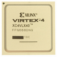
Manufacturer Part Number
XC4VLX40-10FFG668C
Description
IC FPGA VIRTEX-4 40K 668-FCBGA
Manufacturer
Xilinx Inc
Series
Virtex™-4r
Specifications of XC4VLX40-10FFG668C
Total Ram Bits
1769472
Number Of Logic Elements/cells
41472
Number Of Labs/clbs
4608
Number Of I /o
448
Voltage - Supply
1.14 V ~ 1.26 V
Mounting Type
Surface Mount
Operating Temperature
0°C ~ 85°C
Package / Case
668-BBGA, FCBGA
No. Of Logic Blocks
4608
No. Of Macrocells
41472
Family Type
Virtex-4
No. Of Speed Grades
10
No. Of I/o's
448
Clock Management
DCM
Core Supply
RoHS Compliant
Lead Free Status / RoHS Status
Lead free / RoHS Compliant
For Use With
HW-AFX-FF668-400 - BOARD DEV VIRTEX 4 FF668
Number Of Gates
-
Lead Free Status / RoHS Status
Lead free / RoHS Compliant
Other names
122-1492
Available stocks
Company
Part Number
Manufacturer
Quantity
Price
Company:

Part Number:
XC4VLX40-10FFG668C
Manufacturer:
XilinxInc
Quantity:
3 000
Company:
Part Number:
XC4VLX40-10FFG668C
Manufacturer:
Xilinx Inc
Quantity:
10 000


CLB Distributed RAM Switching Characteristics (SLICEM Only)
)
Table 38: CLB Distributed RAM Switching Characteristics
CLB Shift Register Switching Characteristics (SLICEM Only)
)
Table 39: CLB Shift Register Switching Characteristics
DS302 (v3.7) September 9, 2009
Product Specification
Notes:
1.
2.
3.
Notes:
1.
2.
3.
Sequential Delays
Setup and Hold Times Before/After Clock CLK
Clock CLK
Sequential Delays
Setup and Hold Times Before/After Clock CLK
Clock CLK
Symbol
T
T
T
T
T
T
T
T
T
T
T
T
T
T
T
T
T
A Zero “0” Hold Time listing indicates no hold time or a negative hold time. Negative values cannot be guaranteed “best-case,” but if a “0” is listed,
there is no positive hold time.
The values in this column apply to all XC4VFX -12 parts except XC4VFX12 -12. For XC4VFX12 -12 values, use the values in the adjacent
XC4VLX/SX -12 column.
The values in this column apply to all XC4VFX -11 parts.
AS
SHCKO
SHCKOF5
DS
WS
WPH
WPL
WC
REG
REGXB
REGYB
CKSH
REGF5
WS
DS
WPH
WPL
Symbol
SHCKO
/
/
/
/
/
T
T
T
T
T
AH
DH
DH
WH
WH
also represents the CLK to XMUX output. Refer to TRCE report for the CLK to XMUX path.
Clock CLK to X/Y outputs
Clock CLK to XB output via MC15 LUT output
Clock CLK to YB output via MC15 LUT output
Clock CLK to Shiftout
Clock CLK to F5 output
WE input (SR)
BX/BY data inputs (DI)
Minimum Pulse Width, High
Minimum Pulse Width, Low
Clock CLK to X outputs (WE active)
Clock CLK to F5 output (WE active)
BX/BY data inputs (DI)
F/G address inputs
WE input (SR)
Minimum Pulse Width, High
Minimum Pulse Width, Low
Minimum clock period to meet address write cycle time
Description
Description
(3)
www.xilinx.com
Virtex-4 FPGA Data Sheet: DC and Switching Characteristics
XC4VFX
–0.76
–1.12
2.12
1.83
1.84
1.70
2.05
0.87
1.28
0.53
0.55
(2)
-12
XC4VLX/SX
–0.76
–1.11
2.08
1.73
1.74
1.60
2.01
0.85
1.25
0.52
0.54
XC4VFX
–0.90
–0.37
–0.48
1.61
1.53
1.26
0.88
1.10
0.53
0.55
0.76
Speed Grade
(2)
XC4VFX
-12
–0.70
–1.11
1.90
1.92
1.76
XC4VLX/SX
2.19
2.11
0.96
1.45
0.59
0.60
Speed Grade
–0.88
–0.37
–0.47
1.58
1.50
1.23
0.86
1.08
0.52
0.54
0.74
(3)
-11
XC4VLX/SX
–0.70
–1.11
2.19
1.84
1.85
1.70
2.11
0.96
1.45
0.59
0.60
–0.88
–0.34
–0.47
1.77
1.69
1.46
0.97
1.21
0.59
0.60
0.84
ALL DEVICES
-11
–0.88
–0.29
–0.47
–0.62
–1.11
2.08
1.98
1.80
1.13
1.42
0.69
0.70
0.98
-10
2.57
2.16
2.17
1.99
2.47
1.12
1.75
0.69
0.70
ALL
-10
ns, Max
ns, Max
ns, Max
ns, Max
ns, Max
ns, Max
ns, Max
ns, Min
ns, Min
ns, Min
ns, Min
ns, Min
ns, Min
ns, Min
ns, Min
ns, Min
ns, Min
Units
Units
32
Related parts for XC4VLX40-10FFG668C
Image
Part Number
Description
Manufacturer
Datasheet
Request
R

Part Number:
Description:
IC FPGA VIRTEX-4 40K 1148-FBGA
Manufacturer:
Xilinx Inc
Datasheet:

Part Number:
Description:
IC FPGA VIRTEX-4 LX 40K 668FCBGA
Manufacturer:
Xilinx Inc
Datasheet:
Part Number:
Description:
IC FPGA VIRTEX-4 LX 40K 1148FBGA
Manufacturer:
Xilinx Inc
Datasheet:
Part Number:
Description:
IC FPGA VIRTEX-4 LX 40K 1148FBGA
Manufacturer:
Xilinx Inc
Datasheet:
Part Number:
Description:
IC FPGA VIRTEX-4 LX 40K 668FCBGA
Manufacturer:
Xilinx Inc
Datasheet:
Part Number:
Description:
IC FPGA VIRTEX-4 LX 40K 668FCBGA
Manufacturer:
Xilinx Inc
Datasheet:
Part Number:
Description:
IC FPGA VIRTEX-4 LX 40K 1148FBGA
Manufacturer:
Xilinx Inc
Datasheet:
Part Number:
Description:
IC FPGA VIRTEX-4 LX 40K 1148FBGA
Manufacturer:
Xilinx Inc
Datasheet:
Part Number:
Description:
IC FPGA VIRTEX-4LX 668FFBGA
Manufacturer:
Xilinx Inc
Datasheet:
Part Number:
Description:
IC FPGA VIRTEX-4LX 1148FFBGA
Manufacturer:
Xilinx Inc
Datasheet:
Part Number:
Description:
IC FPGA VIRTEX-4LX 668FFBGA
Manufacturer:
Xilinx Inc
Datasheet:
Part Number:
Description:
IC FPGA VIRTEX-4LX 1148FFBGA
Manufacturer:
Xilinx Inc
Datasheet:
Part Number:
Description:
FPGA Virtex®-4 Family 41472 Cells 90nm (CMOS) Technology 1.2V 1148-Pin FCBGA
Manufacturer:
Xilinx Inc
Datasheet:
Part Number:
Description:
FPGA Virtex®-4 Family 41472 Cells 90nm (CMOS) Technology 1.2V 668-Pin FCBGA
Manufacturer:
Xilinx Inc
Datasheet:

Part Number:
Description:
IC CPLD .8K 36MCELL 44-VQFP
Manufacturer:
Xilinx Inc
Datasheet: