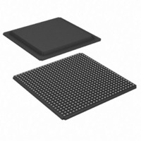
XC2V3000-6FGG676C Xilinx Inc, XC2V3000-6FGG676C Datasheet - Page 11

XC2V3000-6FGG676C
Manufacturer Part Number
XC2V3000-6FGG676C
Description
IC FPGA VIRTEX-II 3M 676-FBGA
Manufacturer
Xilinx Inc
Series
Virtex™-IIr
Datasheet
1.XC2V250-4FGG256C.pdf
(318 pages)
Specifications of XC2V3000-6FGG676C
Number Of Labs/clbs
3584
Total Ram Bits
1769472
Number Of I /o
484
Number Of Gates
3000000
Voltage - Supply
1.425 V ~ 1.575 V
Mounting Type
Surface Mount
Operating Temperature
0°C ~ 85°C
Package / Case
676-BBGA
Lead Free Status / RoHS Status
Lead free / RoHS Compliant
Number Of Logic Elements/cells
-
Available stocks
Company
Part Number
Manufacturer
Quantity
Price
Company:
Part Number:
XC2V3000-6FGG676C
Manufacturer:
Xilinx Inc
Quantity:
10 000
- Current page: 11 of 318
- Download datasheet (3Mb)
The DDR mechanism shown in
ror a copy of the clock on the output. This is useful for prop-
agating a clock along the data that has an identical delay. It
is also useful for multiple clock generation, where there is a
unique clock driver for every clock load. Virtex-II devices
can produce many copies of a clock with very little skew.
Each group of two registers has a clock enable signal (ICE
for the input registers, OCE for the output registers, and
TCE for the 3-state registers). The clock enable signals are
active High by default. If left unconnected, the clock enable
for that storage element defaults to the active state.
Each IOB block has common synchronous or asynchronous
set and reset (SR and REV signals).
SR forces the storage element into the state specified by the
SRHIGH or SRLOW attribute. SRHIGH forces a logic “1”.
SRLOW forces a logic “0”. When SR is used, a second input
(REV) forces the storage element into the opposite state. The
reset condition predominates over the set condition. The ini-
tial state after configuration or global initialization state is
defined by a separate INIT0 and INIT1 attribute. By default,
the SRLOW attribute forces INIT0, and the SRHIGH attribute
forces INIT1.
DS031-2 (v3.5) November 5, 2007
Product Specification
CLOCK
R
D1
D2
CLK1
CLK2
Figure 3
(50/50 duty cycle clock)
Q1
Q2
can be used to mir-
Figure 3: Double Data Rate Registers
DDR MUX
FDDR
www.xilinx.com
Q
For each storage element, the SRHIGH, SRLOW, INIT0,
and INIT1 attributes are independent. Synchronous or
asynchronous set / reset is consistent in an IOB block.
All the control signals have independent polarity. Any
inverter placed on a control input is automatically absorbed.
Each register or latch (independent of all other registers or
latches) (see
•
•
•
•
•
•
•
The synchronous reset overrides a set, and an asynchro-
nous clear overrides a preset.
180° 0°
No set or reset
Synchronous set
Synchronous reset
Synchronous set and reset
Asynchronous set (preset)
Asynchronous reset (clear)
Asynchronous set and reset (preset and clear)
DCM
Virtex-II Platform FPGAs: Functional Description
Figure
D1
D2
CLK1
CLK2
4) can be configured as follows:
Q1
Q2
DDR MUX
FDDR
DS031_26_100900
Q
Module 2 of 4
3
Related parts for XC2V3000-6FGG676C
Image
Part Number
Description
Manufacturer
Datasheet
Request
R

Part Number:
Description:
IC VIRTEX-II FPGA 3M 676-FBGA
Manufacturer:
Xilinx Inc
Datasheet:

Part Number:
Description:
IC VIRTEX-II FPGA 3M 1152-FCBGA
Manufacturer:
Xilinx Inc
Datasheet:

Part Number:
Description:
IC FPGA VIRTEX II 3M 957-FCBGA
Manufacturer:
Xilinx Inc
Datasheet:

Part Number:
Description:
IC FPGA VIRTEX-II 3M 676-FBGA
Manufacturer:
Xilinx Inc
Datasheet:

Part Number:
Description:
IC FPGA VIRTEX II 3M 957-FCBGA
Manufacturer:
Xilinx Inc
Datasheet:

Part Number:
Description:
IC FPGA VIRTEX-II 3M 1152-FBGA
Manufacturer:
Xilinx Inc
Datasheet:

Part Number:
Description:
IC FPGA VIRTEX-II 3M 1152-FBGA
Manufacturer:
Xilinx Inc
Datasheet:

Part Number:
Description:
IC FPGA VIRTEX-II 3M 676-FBGA
Manufacturer:
Xilinx Inc
Datasheet:

Part Number:
Description:
IC FPGA VIRTEX-II 3M 1152-FBGA
Manufacturer:
Xilinx Inc
Datasheet:

Part Number:
Description:
IC FPGA VIRTEX-II 3M 1152-FBGA
Manufacturer:
Xilinx Inc
Datasheet:

Part Number:
Description:
IC FPGA VIRTEX-II 676FGBGA
Manufacturer:
Xilinx Inc
Datasheet:

Part Number:
Description:
IC FPGA VIRTEX-II 728PBGA
Manufacturer:
Xilinx Inc
Datasheet:

Part Number:
Description:
IC FPGA VIRTEX-II 1152FCBGA
Manufacturer:
Xilinx Inc
Datasheet:

Part Number:
Description:
IC FPGA VIRTEX-II 957FCBGA
Manufacturer:
Xilinx Inc
Datasheet:

Part Number:
Description:
IC FPGA VIRTEX-II 957FCBGA
Manufacturer:
Xilinx Inc
Datasheet:


