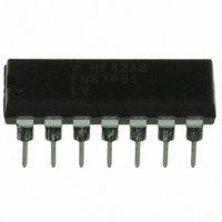
FMS7401LVN14 Fairchild Semiconductor, FMS7401LVN14 Datasheet - Page 41

FMS7401LVN14
Manufacturer Part Number
FMS7401LVN14
Description
IC CTRLR POWER DGTL EEPROM 14DIP
Manufacturer
Fairchild Semiconductor
Datasheet
1.FMS7401LVN.pdf
(81 pages)
Specifications of FMS7401LVN14
Applications
Digital Power Controller
Core Processor
8-Bit
Program Memory Type
EEPROM (1 kB)
Ram Size
64 x 8
Number Of I /o
8
Voltage - Supply
2.7 V ~ 3.6 V
Operating Temperature
-40°C ~ 125°C
Mounting Type
Through Hole
Package / Case
14-DIP (0.300", 7.62mm)
Output Current
5 mA
Input Voltage
2.7 V to 3.6 V
Switching Frequency
2 MHz
Operating Temperature Range
- 40 C to + 125 C
Mounting Style
Through Hole
Lead Free Status / RoHS Status
Lead free / RoHS Compliant
Interface
-
Controller Series
-
Lead Free Status / Rohs Status
Lead free / RoHS Compliant
Other names
FMS7401LVN14_NL
FMS7401LVN14_NL
FMS7401LVN14_NL
7
Timer 0’s main circuit is a 12-bit free running up-counter whose clock source is the main system instruction clock (F
main counter may be used to generate microcontroller hardware interrupts and serve as a prescaler for the Idle and Watchdog
Timers.
After power-up or any system reset, the Timer 0’s 12-bit counter is initialized to 0x000 and continuously increments with each
instruction clock. The 12-bit counter is not memory mapped; therefore, software cannot read or write to the counter registers.
However, software may monitor the Timer 0’s main counter by reading the state of the Timer 0 Pending (T0PND) bit of the
Timer 0 Control (T0CNTRL) memory mapped register.
(a transition from 0xFFF to 0x000) which occurs after every 4,096 cycles. At every overflow, the counter rolls over to 0x000
and continues to increment. In order for software to properly monitor the main counter, the T0PND bit must be cleared before
the next counter overflow.
The T0CNTRL register houses two hardware interrupt enable bits. The WKINTEN register bit is the MIW hardware interrupt
enable bit. For details regarding its usage refer to the
register bit is Timer 0’s microcontroller hardware interrupt (TMRI0) enable bit. If set, hardware interrupts are enabled and
trigger by the T0PND flag.
Timer 0 interrupt service routine until the pending flag is cleared.
The SBIT or RBIT instructions may be used to either set or clear the T0INTEN or WKINTEN bits. The SBIT and RBIT
instructions both take two instruction clock cycles to complete their execution. In the first cycle, all register bits are automati-
cally read to obtain their most current value. In the second cycle, the bit to be set/cleared is given its new value and all bits are
then re-written to the register. Using the SBIT/RBIT instruction to set/clear an enable bit with a pending flag in the same regis-
ter may cause a potential hazard. Software may inadvertently clear a recently triggered pending flag if the trigger happened
during the second phase of the SBIT/RBIT instruction execution. To avoid this condition, the LD instruction must be used to
set or clear the interrupt enable bits. The Timer 0 circuit is designed such that software may not trigger a pending flag by writ-
ing a 1 to a T0PND register bit, it may only be cleared. The action of writing a 1 to a T0PND register bit holds the current bit
value. The action of writing a 0 to a T0PND register bit clears the bit value. Therefore, the “LD T0CNTRL, #083H” instruction
will set both interrupt enable bits without clearing T0PND.
Table 18. Timer 0 Control (T0CNTRL) Register Definitions
7.1
Once the device enters Idle Mode, the microcontroller core and other main circuits are disabled for current conservation. The
Idle Timer will automatically wake the device from Idle Mode, if the MIW has not already done so, after a maximum of 8,192
cycles.
The Idle Timer is a 1-bit extension of the Timer 0’s main 12-bit up-counter. With each overflow of the main counter, the Idle
Timer extension bit is toggled essentially causing the Idle Timer overflow to occur after 8,192 cycles. Once the Idle Timer
overflow flag is triggered, the device wakes from Idle Mode and starts its instruction execution with the next clock cycle.
The Idle Timer overflow flag cannot be monitored by software. Therefore, in order to maximize the time that the device
remains in Idle Mode software must monitor the T0PND flag. Once the T0PND flag is triggered, software may then issue the
Idle Mode command. Software may also loop on the Idle Mode command to extend the average time the device remains in Idle
Mode, thereby reducing the overall current consumption.
7.2
The Watchdog Timer is used to safely recover the device in the rare event of a processor “runaway condition” by issuing a sys-
tem reset. A Watchdog Timer runs continuously with Timer 0’s main 12-bit up-counter; however, a Watchdog Reset will not
REV. 1.0.3 1/24/05
PRODUCT SPECIFICATION
WKINTEN
Timer 0 Circuit
Bit 7
Idle Timer
5
Watchdog Timer
Bit 6
x
2
As long as a Timer 0 pending flag is set, the hardware interrupt will continue to execute software’s
Bit 5
x
T0CNTRL Register (addr. 0xB6)
Bit 4
Multi-input Wakeup Circuit
x
1
The T0PND flag is automatically set with each counter overflow
3
4
Bit 3
x
section of the datasheet. The T0INTEN
Bit 2
x
T0PND
Bit 1
T0INTEN
ICLK
Bit 0
FMS7401L
). The
41


