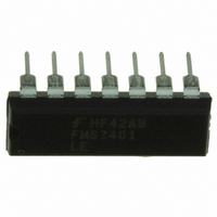
FMS7401LEN14 Fairchild Semiconductor, FMS7401LEN14 Datasheet - Page 55

FMS7401LEN14
Manufacturer Part Number
FMS7401LEN14
Description
IC CTRLR POWER DGTL EEPROM 14DIP
Manufacturer
Fairchild Semiconductor
Datasheet
1.FMS7401LVN.pdf
(81 pages)
Specifications of FMS7401LEN14
Applications
Digital Power Controller
Core Processor
8-Bit
Program Memory Type
EEPROM (1 kB)
Ram Size
64 x 8
Number Of I /o
8
Voltage - Supply
2.7 V ~ 3.6 V
Operating Temperature
-40°C ~ 85°C
Mounting Type
Through Hole
Package / Case
14-DIP (0.300", 7.62mm)
Output Current
5 mA
Input Voltage
2.7 V to 3.6 V
Switching Frequency
2 MHz
Operating Temperature Range
- 40 C to + 85 C
Mounting Style
Through Hole
Lead Free Status / RoHS Status
Lead free / RoHS Compliant
Interface
-
Controller Series
-
Lead Free Status / Rohs Status
Lead free / RoHS Compliant
Other names
FMS7401LEN14_NL
FMS7401LEN14_NL
FMS7401LEN14_NL
Available stocks
Company
Part Number
Manufacturer
Quantity
Price
Company:
Part Number:
FMS7401LEN14
Manufacturer:
Rohm
Quantity:
21 626
FMS7401L
prior to leaving the factory with the appropriate calibration value and with the ports configured as tri-state inputs. In program-
ming mode, the default port configuration may be changed; however, be sure to maintain the factory current source calibration
value since writes to a single register must affect all bits.
The Initialization Registers 1, 2, 3 and 4 can be read from and written to while in programming mode. However, re-trimming
the internal oscillator and re-calibrating the analog circuits once the device has left the factory is discouraged and will void all
device guarantees.
Table 26. Initialization Register 1 Bit Definitions
Table 27. Initialization Register 3 Bit Definitions
Table 28. Initialization Register 4 Bit Definitions
55
Initialization Register 3 (volatile/non-volatile addr. 0xD0, 0xD1)
Initialization Register 4 (volatile/non-volatile addr. 0xD3, 0xD4)
T1HS_DIR
CLK_ADJ
unused
Bit 7
Bit 7
Bit 7
(6:5)
(4:0)
(5:3)
(2:0)
(7)
(6)
(4)
(3)
(2)
(1)
(0)
(7)
COMP_TRIM
T1HS2_LEV
BOR_TRIM
ISOURCE_TRIM
CLKADJ
CMODE
CMODE
BOREN
WDEN
WDIS
unused
RDIS
T1HSx_LEV
Bit 6
UBD
Bit 6
Bit 6
T1HS_DIR
6
6
When set, the internal clock trimming register (volatile Initialization Register 2, Addr. 0xBA) can be
accessed by the core in order to modify the internal clock frequency.
Clock mode select: 0 = Internal Oscillator, 1 = External Oscillator
If set, the on-chip processor Watchdog Timer resets are enabled.
If set, the on-chip Brown-out Reset comparator circuit is enabled.
If set, write access of the upper 32 bytes of the data EEPROM (0x60-0x7F) is disabled in both
programming and normal mode.
If set, write access of the device memory is permanently disabled while in programming mode.
If set, read access of the device memory is permanently disabled while in programming mode.
Initialization Register 1 (volatile/non-volatile addr. 0xB9, 0xBB)
These three bits allow for the calibration of the Brown-out Reset comparator circuit.
These three bits allow for the calibration of the Programmable Comparator’s upper range circuit.
T1HS1_LEV
unused
Bit 5
Bit 5
Bit 5
Initializes during reset, the T1HS1 (G0) and T1HS2 (G5) I/O ports both either inputs or outputs.
This bit shadows directly to bits 0 and 5 of PORTGC.
Initializes during reset, the individual T1HS1 (G0) and T1HS2 (G5) I/O port level. These bits
shadow directly to bits 0 and 5 of PORTGD.
These five bits allow for the calibration of internal current source generator.
BOR_TRIM
WDEN
Bit 4
Bit 4
Bit 4
1,2
BOREN
Bit 3
Bit 3
Bit 3
ISOURCE_TRIM[4:0]
Bit 2
UBD
Bit 2
Bit 2
COMP_TRIM
WDIS
PRODUCT SPECIFICATION
Bit 1
Bit 1
Bit 1
6
REV. 1.0.3 1/24/05
RDIS
Bit 0
Bit 0
Bit 0
2
2
6


