CY8C20496A-24LQXI Cypress Semiconductor Corp, CY8C20496A-24LQXI Datasheet - Page 9
CY8C20496A-24LQXI
Manufacturer Part Number
CY8C20496A-24LQXI
Description
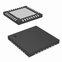
MCU 16K FLASH 2K SRAM 32UQFN
Manufacturer
Cypress Semiconductor Corp
Series
CapSense® Controllersr
Datasheet
1.CY8C20536A-24PVXI.pdf
(38 pages)
Specifications of CY8C20496A-24LQXI
Program Memory Type
FLASH (16 kB)
Package / Case
32-UQFN Exposed Pad
Applications
Capacitive Sensing
Core Processor
M8C
Controller Series
CY8C20xx6A
Ram Size
2K x 8
Interface
I²C, SPI, USB
Number Of I /o
28
Voltage - Supply
1.71 V ~ 5.5 V
Operating Temperature
-40°C ~ 85°C
Mounting Type
Surface Mount
Processor Series
CY8C20x96A
Core
M8C
Data Bus Width
8 bit
Data Ram Size
2 KB
Interface Type
I2C, SPI
Maximum Clock Frequency
24 MHz
Number Of Programmable I/os
22
Number Of Timers
3
Operating Supply Voltage
1.71 V to 5.5 V
Maximum Operating Temperature
+ 85 C
Mounting Style
SMD/SMT
Development Tools By Supplier
CY3280-20X66
Minimum Operating Temperature
- 40 C
Program Memory Size
16 KB
Lead Free Status / RoHS Status
Lead free / RoHS Compliant
For Use With
770-1000 - ISP 4PORT FOR CYPRESS PSOC MCU
Lead Free Status / Rohs Status
Lead free / RoHS Compliant


24-Pin QFN
Table 3. Pin Definitions - CY8C20336A, CY8C20346A
Document Number: 001-54459 Rev. **
Note
1
2
3
4
5
6
7
8
9
10
11
12
13
14
15
16
17
18
19
20
21
22
23
24
CP
LEGEND A = Analog, I = Input, O = Output, OH = 5 mA High Output Drive, R = Regulated Output.
Pin
No.
3. The center pad (CP) on the QFN package must be connected to ground (Vss) for best mechanical, thermal, and electrical performance. If not connected to ground, it
must be electrically floated and not connected to any other signal.
Digital Analog
IOHR
IOHR
IOHR
IOHR
IOHR
IOHR
IOHR
IOHR
IOH
IOH
IOH
IOH
IOH
IOH
IOH
IOH
I/O
I/O
I/O
I/O
Power
Power
Power
Type
Input
I
I
I
I
I
I
I
I
I
I
I
I
I
I
I
I
I
I
I
I
Name
P2[5]
P2[3]
P2[1]
P1[7]
P1[5]
P1[3]
P1[1]
NC
Vss
P1[0]
P1[2]
P1[4]
P1[6]
XRES
P2[0]
P0[0]
P0[2]
P0[4]
P0[6]
Vdd
P0[7]
P0[5]
P0[3]
P0[1]
Vss
Crystal output (XOut)
Crystal input (XIn)
I2C SCL, SPI SS
I2C SDA, SPI MISO
SPI CLK
ISSP CLK
MOSI
No connection
Ground connection
ISSP DATA
CLK
Optional external clock input
(EXTCLK)
Active high external reset with
internal pull down
Supply voltage
Integrating input
Integrating input
Center pad must be connected
to ground
Description
[1]
[1]
, I2C SCL, SPI
, I2C SDA, SPI
[2, 3]
Figure 3. CY8C20336A, CY8C20346A PSoC Device
AI, I2C SDA, SPI MISO, P1[5]
AI, I2C SCL, SPI SS, P1[7]
AI, SPI CLK, P1[3]
AI, XOut, P2[5]
AI, XIn, P2[3]
CY8C20X36A/46A/66A/96A
AI, P2[1]
1
4
2
3
5
6
(Top View)
QFN
18
13
17
16
15
14
P0[4], AI
P0[2], AI
P0[0], AI
P2[0], AI
P1[6], AI
XRES
Page 9 of 38
[+] Feedback
Related parts for CY8C20496A-24LQXI
Image
Part Number
Description
Manufacturer
Datasheet
Request
R

Part Number:
Description:
CY8C20496A-24LQXIT
Manufacturer:
Cypress Semiconductor Corp

Part Number:
Description:
Manufacturer:
Cypress Semiconductor Corp
Datasheet:
Part Number:
Description:
Manufacturer:
Cypress Semiconductor Corp
Datasheet:
Part Number:
Description:
Manufacturer:
Cypress Semiconductor Corp
Datasheet:
Part Number:
Description:
Manufacturer:
Cypress Semiconductor Corp
Datasheet:
Part Number:
Description:
Manufacturer:
Cypress Semiconductor Corp
Datasheet: