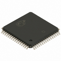
CY7C53150-20AXI Cypress Semiconductor Corp, CY7C53150-20AXI Datasheet - Page 7

CY7C53150-20AXI
Manufacturer Part Number
CY7C53150-20AXI
Description
IC PROCESSOR NEURON 64LQFP
Manufacturer
Cypress Semiconductor Corp
Series
Neuron®r
Datasheet
1.CY7C53150-20AXI.pdf
(16 pages)
Specifications of CY7C53150-20AXI
Package / Case
64-LQFP
Applications
Network Processor
Core Processor
Pipelined
Program Memory Type
FLASH (512 B)
Controller Series
CY7C531xx
Ram Size
2K x 8
Interface
Serial
Number Of I /o
19
Voltage - Supply
4.5 V ~ 5.5 V
Operating Temperature
-40°C ~ 85°C
Mounting Type
Surface Mount
Product
Network Processor
Frequency
20 MHz
Maximum Operating Temperature
+ 85 C
Minimum Operating Temperature
- 40 C
Mounting Style
SMD/SMT
Operating Supply Voltage (typ)
5V
Operating Supply Voltage (max)
5.5V
Operating Supply Voltage (min)
4.5V
Mounting
Surface Mount
Operating Temperature (max)
85C
Operating Temperature (min)
-40C
Operating Temperature Classification
Industrial
Lead Free Status / RoHS Status
Lead free / RoHS Compliant
Lead Free Status / RoHS Status
Lead free / RoHS Compliant, Lead free / RoHS Compliant
Other names
428-2912
CY7C53150-20AXI
CY7C53150-20AXI
Available stocks
Company
Part Number
Manufacturer
Quantity
Price
Company:
Part Number:
CY7C53150-20AXI
Manufacturer:
OMRON
Quantity:
3 000
Company:
Part Number:
CY7C53150-20AXI
Manufacturer:
CY
Quantity:
62
Company:
Part Number:
CY7C53150-20AXI
Manufacturer:
CYPRESS
Quantity:
99
Company:
Part Number:
CY7C53150-20AXI
Manufacturer:
Cypress Semiconductor Corp
Quantity:
10 000
Part Number:
CY7C53150-20AXI
Manufacturer:
CIRRUS
Quantity:
20 000
Company:
Part Number:
CY7C53150-20AXIT
Manufacturer:
Cypress Semiconductor Corp
Quantity:
10 000
Programmable Hysteresis Values
(Expressed as differential peak-to-peak voltages in terms of V
Programmable Glitch Filter Values
(Receiver (end-to-end) filter values expressed as transient pulse
suppression times)
Notes
Document #: 38-10001 Rev. *G
6. Hysteresis values are on the condition that the input signal swing is 200 mV greater than the programmed value.
7. Must be disabled if data rate is 1.25 Mbps or greater.
8. Receiver input, V
9. CPO and CP1 inputs each 0.60 Vp – p, 1.25 MHz sine wave 180° out of phase with each other as shown in
10. t
Hysteresis
Filter (F)
PLH
0
1
2
3
: Time from input switching states from low to high to output switching states. t
0
1
2
3
4
5
6
7
[6]
D
= V
Min
120
240
480
0.019 V
0.040 V
0.061 V
0.081 V
0.101 V
0.121 V
0.142 V
0.162 V
10
V
CP0
hys
– V
Min
CP1
DD
DD
DD
DD
DD
DD
DD
DD
, at least 200 mV greater than hysteresis levels. See
1500
Typ
410
800
75
0.027 V
0.054 V
0.081 V
0.108 V
0.135 V
0.162 V
0.189 V
0.216 V
V
hys
Typ
[7]
DD
DD
DD
DD
DD
DD
DD
DD
1350
2600
Max
140
700
0.035 V
0.068 V
0.101 V
0.135 V
0.169 V
0.203 V
0.236 V
0.270 V
V
hys
Max
Unit
ns
ns
ns
ns
DD
DD
DD
DD
DD
DD
DD
DD
DD
)
PHL
Receiver
(Worst case across hysteresis)
Differential Receiver (End-to-End) Absolute
Symmetry
: Time from input switching states from high to low to output switching states.
Filter (F)
Figure
Filter (F)
0
0
1
2
3
3.
V
Figure 3. Receiver Input Waveform
[8]
DD
CP0
CP1
⎮
[9, 10]
V
(End-to-End) Absolute Asymmetry
/2
CP0 – CP1
hys
Hysteresis (H)
+ 200 mV
Figure
0
CY7C53150, CY7C53120
⎮
10. V
≥
Max (t
DD
= 5.00 V ± 5%.
≤ 3 ns
PLH
150
250
400
35
Max (t
– t
PHL
PLH
24
)
– t
PHL
Page 7 of 16
)
Unit
Unit
ns
ns
ns
ns
ns
[+] Feedback


