MPC8250AVRIHBC Freescale Semiconductor, MPC8250AVRIHBC Datasheet - Page 3
MPC8250AVRIHBC
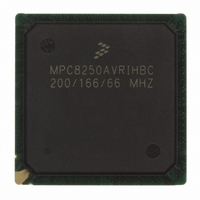
Manufacturer Part Number
MPC8250AVRIHBC
Description
IC MPU POWERQUICC II 516-PBGA
Manufacturer
Freescale Semiconductor
Datasheet
1.MPC8250AVRIHBC.pdf
(62 pages)
Specifications of MPC8250AVRIHBC
Processor Type
MPC82xx PowerQUICC II 32-bit
Speed
200MHz
Voltage
1.8V
Mounting Type
Surface Mount
Package / Case
516-PBGA
Processor Series
MPC8xxx
Core
603e
Data Bus Width
32 bit
Maximum Clock Frequency
200 MHz
Maximum Operating Temperature
+ 105 C
Mounting Style
SMD/SMT
Minimum Operating Temperature
0 C
Family Name
MPC82XX
Device Core
PowerQUICC II
Device Core Size
32b
Frequency (max)
200MHz
Instruction Set Architecture
RISC
Supply Voltage 1 (typ)
1.8V
Operating Supply Voltage (max)
1.9V
Operating Supply Voltage (min)
1.7V
Operating Temp Range
0C to 105C
Operating Temperature Classification
Commercial
Mounting
Surface Mount
Pin Count
516
Package Type
TEPBGA
Leaded Process Compatible
Yes
Rohs Compliant
Yes
Peak Reflow Compatible (260 C)
Yes
For Use With
CWH-PPC-8248N-VE - KIT EVAL SYSTEM QUICCSTART 8248
Lead Free Status / RoHS Status
Lead free / RoHS Compliant
Features
-
Lead Free Status / Rohs Status
Lead free / RoHS Compliant
Available stocks
Company
Part Number
Manufacturer
Quantity
Price
Company:

Part Number:
MPC8250AVRIHBC
Manufacturer:
MOTOLOLA
Quantity:
875
Company:
Part Number:
MPC8250AVRIHBC
Manufacturer:
Freescale Semiconductor
Quantity:
10 000


Freescale Semiconductor
•
•
•
•
•
•
•
— Supports bus snooping for data cache coherency
— Floating-point unit (FPU)
Separate power supply for internal logic (1.8 V) and for I/O (3.3V)
Separate PLLs for G2 core and for the CPM
— G2 core and CPM can run at different frequencies for power/performance optimization
— Internal core/bus clock multiplier that provides 1.5:1, 2:1, 2.5:1, 3:1, 3.5:1, 4:1, 5:1, 6:1 ratios
— Internal CPM/bus clock multiplier that provides 2:1, 2.5:1, 3:1, 3.5:1, 4:1, 5:1, 6:1 ratios
64-bit data and 32-bit address 60x bus
— Bus supports multiple master designs
— Supports single- and four-beat burst transfers
— 64-, 32-, 16-, and 8-bit port sizes controlled by on-chip memory controller
— Supports data parity or ECC and address parity
32-bit data and 18-bit address local bus
— Single-master bus, supports external slaves
— Eight-beat burst transfers
— 32-, 16-, and 8-bit port sizes controlled by on-chip memory controller
60x-to-PCI bridge
— Programmable host bridge and agent
— 32-bit data bus, 66 MHz, 3.3 V
— Synchronous and asynchronous 60x and PCI clock modes
— All internal address space available to external PCI host
— DMA for memory block transfers
— PCI-to-60x address remapping
System interface unit (SIU)
— Clock synthesizer
— Reset controller
— Real-time clock (RTC) register
— Periodic interrupt timer
— Hardware bus monitor and software watchdog timer
— IEEE 1149.1™ JTAG test access port
Twelve-bank memory controller
— Glueless interface to SRAM, page mode SDRAM, DRAM, EPROM, Flash and other user-
— Byte write enables and selectable parity generation
— 32-bit address decodes with programmable bank size
— Three user programmable machines, general-purpose chip-select machine, and page-mode
— Byte selects for 64 bus width (60x) and byte selects for 32 bus width (local)
definable peripherals
pipeline SDRAM machine
MPC8250 Hardware Specifications, Rev. 2
Features
3
Related parts for MPC8250AVRIHBC
Image
Part Number
Description
Manufacturer
Datasheet
Request
R

Part Number:
Description:
Manufacturer:
Freescale Semiconductor, Inc
Datasheet:
Part Number:
Description:
Manufacturer:
Freescale Semiconductor, Inc
Datasheet:
Part Number:
Description:
Manufacturer:
Freescale Semiconductor, Inc
Datasheet:
Part Number:
Description:
Manufacturer:
Freescale Semiconductor, Inc
Datasheet:
Part Number:
Description:
Manufacturer:
Freescale Semiconductor, Inc
Datasheet:
Part Number:
Description:
Manufacturer:
Freescale Semiconductor, Inc
Datasheet:
Part Number:
Description:
Manufacturer:
Freescale Semiconductor, Inc
Datasheet:
Part Number:
Description:
Manufacturer:
Freescale Semiconductor, Inc
Datasheet:
Part Number:
Description:
Manufacturer:
Freescale Semiconductor, Inc
Datasheet:
Part Number:
Description:
Manufacturer:
Freescale Semiconductor, Inc
Datasheet:
Part Number:
Description:
Manufacturer:
Freescale Semiconductor, Inc
Datasheet:
Part Number:
Description:
Manufacturer:
Freescale Semiconductor, Inc
Datasheet:
Part Number:
Description:
Manufacturer:
Freescale Semiconductor, Inc
Datasheet:
Part Number:
Description:
Manufacturer:
Freescale Semiconductor, Inc
Datasheet:
Part Number:
Description:
Manufacturer:
Freescale Semiconductor, Inc
Datasheet: