MPC8347VRADDB Freescale Semiconductor, MPC8347VRADDB Datasheet - Page 12
MPC8347VRADDB
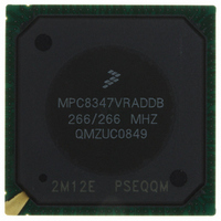
Manufacturer Part Number
MPC8347VRADDB
Description
IC MPU POWERQUICC II 620-PBGA
Manufacturer
Freescale Semiconductor
Series
PowerQUICC II PROr
Specifications of MPC8347VRADDB
Processor Type
MPC83xx PowerQUICC II Pro 32-Bit
Speed
266MHz
Voltage
1.2V
Mounting Type
Surface Mount
Package / Case
620-PBGA
Processor Series
MPC8xxx
Core
e300
Data Bus Width
32 bit
Development Tools By Supplier
MPC8349E-MITXE
Maximum Clock Frequency
266 MHz
Maximum Operating Temperature
+ 105 C
Mounting Style
SMD/SMT
I/o Voltage
1.8 V, 2.5 V, 3.3 V
Minimum Operating Temperature
0 C
Core Size
32 Bit
Program Memory Size
64KB
Cpu Speed
266MHz
Embedded Interface Type
I2C, SPI, USB, UART
Digital Ic Case Style
BGA
No. Of Pins
672
Rohs Compliant
Yes
Lead Free Status / RoHS Status
Lead free / RoHS Compliant
Features
-
Lead Free Status / Rohs Status
Lead free / RoHS Compliant
Available stocks
Company
Part Number
Manufacturer
Quantity
Price
Company:

Part Number:
MPC8347VRADDB
Manufacturer:
Freescale Semiconductor
Quantity:
135
Company:
Part Number:
MPC8347VRADDB
Manufacturer:
Freescale Semiconductor
Quantity:
10 000


Clock Input Timing
4
This section provides the clock input DC and AC electrical characteristics for the device.
4.1
Table 6
4.2
The primary clock source for the MPC8347EA can be one of two inputs, CLKIN or PCI_CLK, depending
on whether the device is configured in PCI host or PCI agent mode.
(CLKIN/PCI_CLK) AC timing specifications for the device.
12
Input high voltage
Input low voltage
CLKIN input current
PCI_SYNC_IN input current
PCI_SYNC_IN input current
CLKIN/PCI_CLK frequency
CLKIN/PCI_CLK cycle time
CLKIN/PCI_CLK rise and fall time
CLKIN/PCI_CLK duty cycle
CLKIN/PCI_CLK jitter
Notes:
1. Caution: The system, core, USB, security, and TSEC must not exceed their respective maximum or minimum operating
2. Rise and fall times for CLKIN/PCI_CLK are measured at 0.4 and 2.7 V.
3. Timing is guaranteed by design and characterization.
4. This represents the total input jitter—short term and long term—and is guaranteed by design.
5. The CLKIN/PCI_CLK driver’s closed loop jitter bandwidth should be < 500 kHz at –20 dB. The bandwidth must be set low to
6. Spread spectrum clocking is allowed with 1% input frequency down-spread at maximum 50 KHz modulation rate regardless
frequencies.
allow cascade-connected PLL-based devices to track CLKIN drivers with the specified jitter.
of input frequency.
Clock Input Timing
provides the clock input (CLKIN/PCI_SYNC_IN) DC timing specifications for the MPC8347EA.
Parameter
DC Electrical Characteristics
AC Electrical Characteristics
MPC8347EA PowerQUICC II Pro Integrated Host Processor Hardware Specifications, Rev. 11
Parameter/Condition
OV
0.5 V ≤V
Table 7. CLKIN AC
Table 6. CLKIN DC Timing Specifications
DD
0 V ≤ V
0 V ≤ V
– 0.5 V ≤ V
Condition
IN
IN
≤ OV
IN
—
—
≤ 0.5 V or
≤ OV
DD
t
IN
KHK
Symbol
t
– 0.5 V
f
KH
DD
≤ OV
t
CLKIN
CLKIN
/t
—
, t
CLKIN
Timing Specifications
KL
DD
Symbol
Min
0.6
15
40
—
—
V
V
I
I
I
IN
IN
IN
IH
IL
Table 7
Typical
1.0
—
—
—
—
–0.3
Min
2.7
—
—
—
provides the clock input
±150
Max
2.3
66
60
—
Freescale Semiconductor
OV
DD
Max
±10
±10
±50
0.4
MHz
Unit
+ 0.3
ns
ns
ps
%
Notes
Unit
1, 6
4, 5
μA
μA
μA
—
V
V
2
3
Related parts for MPC8347VRADDB
Image
Part Number
Description
Manufacturer
Datasheet
Request
R

Part Number:
Description:
Integrated Host Processor Hardware Specifications
Manufacturer:
FREESCALE [Freescale Semiconductor, Inc]
Datasheet:

Part Number:
Description:
Manufacturer:
Freescale Semiconductor, Inc
Datasheet:
Part Number:
Description:
Manufacturer:
Freescale Semiconductor, Inc
Datasheet:
Part Number:
Description:
Manufacturer:
Freescale Semiconductor, Inc
Datasheet:
Part Number:
Description:
Manufacturer:
Freescale Semiconductor, Inc
Datasheet:
Part Number:
Description:
Manufacturer:
Freescale Semiconductor, Inc
Datasheet:
Part Number:
Description:
Manufacturer:
Freescale Semiconductor, Inc
Datasheet:
Part Number:
Description:
Manufacturer:
Freescale Semiconductor, Inc
Datasheet:
Part Number:
Description:
Manufacturer:
Freescale Semiconductor, Inc
Datasheet:
Part Number:
Description:
Manufacturer:
Freescale Semiconductor, Inc
Datasheet:
Part Number:
Description:
Manufacturer:
Freescale Semiconductor, Inc
Datasheet:
Part Number:
Description:
Manufacturer:
Freescale Semiconductor, Inc
Datasheet:
Part Number:
Description:
Manufacturer:
Freescale Semiconductor, Inc
Datasheet:
Part Number:
Description:
Manufacturer:
Freescale Semiconductor, Inc
Datasheet:
Part Number:
Description:
Manufacturer:
Freescale Semiconductor, Inc
Datasheet: