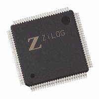
EZ80190AZ050EG Zilog, EZ80190AZ050EG Datasheet - Page 66

EZ80190AZ050EG
Manufacturer Part Number
EZ80190AZ050EG
Description
IC WEBSERVER 50MHZ XTEMP 100LQFP
Manufacturer
Zilog
Datasheet
1.EZ80190AZ050SG.pdf
(221 pages)
Specifications of EZ80190AZ050EG
Processor Type
eZ80
Features
High Speed, Single-Cycle Instruction-Fetch
Speed
50MHz
Voltage
3.3V
Mounting Type
Surface Mount
Package / Case
100-LQFP
Processor Series
EZ80190x
Core
eZ80
Data Bus Width
8 bit
Program Memory Type
ROMLess
Data Ram Size
8 KB
Interface Type
I2C, IrDA, SPI, UART
Maximum Clock Frequency
50 MHz
Number Of Programmable I/os
32
Number Of Timers
6
Operating Supply Voltage
3 V to 3.6 V
Maximum Operating Temperature
+ 70 C
Mounting Style
SMD/SMT
Minimum Operating Temperature
0 C
Lead Free Status / RoHS Status
Lead free / RoHS Compliant
Other names
269-3865
EZ80190AZ050EG
EZ80190AZ050EG
Available stocks
Company
Part Number
Manufacturer
Quantity
Price
Company:
Part Number:
EZ80190AZ050EG
Manufacturer:
TYCO
Quantity:
120
Company:
Part Number:
EZ80190AZ050EG
Manufacturer:
Zilog
Quantity:
70
- Current page: 66 of 221
- Download datasheet (4Mb)
PS006614-1208
Table 18. Chip Select x Lower Bound Register (CS0_LBR = A8h, CS1_LBR = ABh, CS2_LBR
Chip Select x Upper Bound Register
Table 19. Chip Select x Upper Bound Register
Bit
Reset
CPU Access
Note: R/W = Read/Write.
Bit
Position
[7:0]
CS_LBR
Bit
CS0 Reset
CS1 Reset
CS2 Reset
CS3 Reset
CPU Access
Note: R/W = Read/Write.
For Memory Chip Selects, the Chip Select x Upper Bound register, listed in
defines the upper bound of the address range for which the corresponding Chip Select (if
enabled) can be active. For I/O Chip Selects, this register produces no effect. The reset
state for the Chip Select 0 Upper Bound register is
Chip Select upper bound registers is
Value Description
00h–
FFh
For Memory Chip Selects (CS_io = 0)
This bit specifies the lower bound of the Chip Select address
range. The upper byte of the address bus, ADDR[23:16], is
compared to the values contained in these registers for
determining if a Memory Chip Select signal should be generated.
For I/O Chip Selects (CS_io = 1)
This bit specifies the Chip Select address value. ADDR[11:4] is
compared to the values contained in these registers for
determining if an I/O Chip Select signal should be generated.
R/W
R/W
7
0
7
1
0
0
0
CS2_UBR = AFh, CS3_UBR = B2h)
R/W
R/W
6
0
6
1
0
0
0
= AEh, CS3_LBR = B1h)
R/W
R/W
5
0
5
1
0
0
0
00h
.
R/W
R/W
4
0
4
1
0
0
0
(CS0_UBR = A9h, CS1_UBR = ACh,
FFh
R/W
R/W
3
0
3
1
0
0
0
, while the reset state for the 3 other
R/W
R/W
2
0
2
1
0
0
0
Chip Selects and Wait States
Product Specification
R/W
R/W
1
0
1
1
0
0
0
R/W
R/W
Table
0
0
0
1
0
0
0
eZ80190
19,
56
Related parts for EZ80190AZ050EG
Image
Part Number
Description
Manufacturer
Datasheet
Request
R

Part Number:
Description:
Communication Controllers, ZILOG INTELLIGENT PERIPHERAL CONTROLLER (ZIP)
Manufacturer:
Zilog, Inc.
Datasheet:

Part Number:
Description:
KIT DEV FOR Z8 ENCORE 16K TO 64K
Manufacturer:
Zilog
Datasheet:

Part Number:
Description:
KIT DEV Z8 ENCORE XP 28-PIN
Manufacturer:
Zilog
Datasheet:

Part Number:
Description:
DEV KIT FOR Z8 ENCORE 8K/4K
Manufacturer:
Zilog
Datasheet:

Part Number:
Description:
KIT DEV Z8 ENCORE XP 28-PIN
Manufacturer:
Zilog
Datasheet:

Part Number:
Description:
DEV KIT FOR Z8 ENCORE 4K TO 8K
Manufacturer:
Zilog
Datasheet:

Part Number:
Description:
CMOS Z8 microcontroller. ROM 16 Kbytes, RAM 256 bytes, speed 16 MHz, 32 lines I/O, 3.0V to 5.5V
Manufacturer:
Zilog, Inc.
Datasheet:

Part Number:
Description:
Low-cost microcontroller. 512 bytes ROM, 61 bytes RAM, 8 MHz
Manufacturer:
Zilog, Inc.
Datasheet:

Part Number:
Description:
Z8 4K OTP Microcontroller
Manufacturer:
Zilog, Inc.
Datasheet:

Part Number:
Description:
CMOS SUPER8 ROMLESS MCU
Manufacturer:
Zilog, Inc.
Datasheet:

Part Number:
Description:
SL1866 CMOSZ8 OTP Microcontroller
Manufacturer:
Zilog, Inc.
Datasheet:

Part Number:
Description:
SL1866 CMOSZ8 OTP Microcontroller
Manufacturer:
Zilog, Inc.
Datasheet:

Part Number:
Description:
OTP (KB) = 1, RAM = 125, Speed = 12, I/O = 14, 8-bit Timers = 2, Comm Interfaces Other Features = Por, LV Protect, Voltage = 4.5-5.5V
Manufacturer:
Zilog, Inc.
Datasheet:

Part Number:
Description:
Manufacturer:
Zilog, Inc.
Datasheet:


