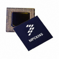
MPC8245LVV266D Freescale Semiconductor, MPC8245LVV266D Datasheet - Page 22

MPC8245LVV266D
Manufacturer Part Number
MPC8245LVV266D
Description
IC MPU 32BIT 266MHZ PPC 352-TBGA
Manufacturer
Freescale Semiconductor
Series
PowerQUICC IIr
Datasheet
1.MPC8245LZU266D.pdf
(68 pages)
Specifications of MPC8245LVV266D
Processor Type
MPC82xx PowerQUICC II 32-bit
Speed
266MHz
Voltage
1.8V
Mounting Type
Surface Mount
Package / Case
352-TBGA
Core Size
32 Bit
Program Memory Size
32KB
Cpu Speed
266MHz
Embedded Interface Type
I2C, UART
Digital Ic Case Style
TBGA
No. Of Pins
352
Supply Voltage Range
1.7V To 2.1V
Rohs Compliant
Yes
Lead Free Status / RoHS Status
Lead free / RoHS Compliant
Features
-
Available stocks
Company
Part Number
Manufacturer
Quantity
Price
Company:
Part Number:
MPC8245LVV266D
Manufacturer:
Freescal
Quantity:
672
Company:
Part Number:
MPC8245LVV266D
Manufacturer:
Freescale Semiconductor
Quantity:
10 000
Part Number:
MPC8245LVV266D
Manufacturer:
FREESCALE
Quantity:
20 000
Electrical and Thermal Characteristics
Figure 11
PCI_SYNC_IN, respectively.
22
SDRAM_SYNC_IN
Shown in 2:1 Mode
Notes:
VM = Midpoint voltage (1.4 V).
10b-d = Input signals valid timing.
11a = Input hold time of SDRAM_SYNC_IN to memory.
12b-d = sys_logic_clk to output valid timing.
13b = Output hold time for non-PCI signals.
14b = SDRAM-SYNC_IN to output high-impedance timing for non-PCI signals.
T
os
PCI_SYNC_IN
Inputs/Outputs
(after DLL locks)
and
PCI_SYNC_IN
Inputs/Outputs
= Offset timing required to align sys_logic_clk with SDRAM_SYNC_IN. The SDRAM_SYNC_IN signal
sys_logic_clk
is adjusted by the DLL to accommodate for internal delay. This causes SDRAM_SYNC_IN to appear
before sys_logic_clk once the DLL locks.
Figure 12
Figure 11. Input/Output Timing Diagram Referenced to SDRAM_SYNC_IN
Memory
Figure 12. Input/Output Timing Diagram Referenced to PCI_SYNC_IN
PCI
MPC8245 Integrated Processor Hardware Specifications, Rev. 10
show the input/output timing diagrams referenced to SDRAM_SYNC_IN and
10a
10b-d
Input Timing
T
Input Timing
os
0.4 × OV
VM
VM
VM
OV
DD
DD
÷ 2
11a
11c
2.0 V
0.8 V
OV
2.0 V
0.8 V
12a
DD
VM
12b-d
÷ 2
Output Timing
0.615 × OV
0.285 × OV
Output Timing
14a
13a
DD
DD
14b
13b
OV
Freescale Semiconductor
DD
VM
÷ 2


