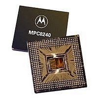
XPC8240RZU250E Freescale Semiconductor, XPC8240RZU250E Datasheet - Page 4

XPC8240RZU250E
Manufacturer Part Number
XPC8240RZU250E
Description
MCU HOST PROCESSOR 352-TBGA
Manufacturer
Freescale Semiconductor
Series
PowerQUICC IIr
Specifications of XPC8240RZU250E
Processor Type
MPC82xx PowerQUICC II 32-bit
Speed
200MHz
Voltage
2.5V
Mounting Type
Surface Mount
Package / Case
352-TBGA
Core Size
32 Bit
Program Memory Size
32KB
Cpu Speed
250MHz
Embedded Interface Type
I2C
Digital Ic Case Style
TBGA
No. Of Pins
352
Supply Voltage Range
2.5V To 2.75V
Rohs Compliant
No
Family Name
MPC82XX
Device Core Size
32b
Frequency (max)
250MHz
Instruction Set Architecture
RISC
Supply Voltage 1 (typ)
2.625/2.6255V
Operating Supply Voltage (max)
2.75625/2.756775V
Operating Supply Voltage (min)
2.49375/2.494225V
Operating Temp Range
0C to 105C
Operating Temperature Classification
Commercial
Mounting
Surface Mount
Pin Count
352
Package Type
TBGA
Lead Free Status / RoHS Status
Contains lead / RoHS non-compliant
Features
-
Lead Free Status / Rohs Status
Not Compliant
Available stocks
Company
Part Number
Manufacturer
Quantity
Price
Company:
Part Number:
XPC8240RZU250E
Manufacturer:
MOT
Quantity:
12 388
Company:
Part Number:
XPC8240RZU250E
Manufacturer:
MOTOLOLA
Quantity:
513
Company:
Part Number:
XPC8240RZU250E
Manufacturer:
Freescale Semiconductor
Quantity:
10 000
Part Number:
XPC8240RZU250E
Manufacturer:
FREESCALE
Quantity:
20 000
PLL Configurations
PLL Configurations
1.5
The MPC8240 internal PLLs are configured by the PLL_CFG[0:4] signals. For a given PCI_SYNC_IN
(PCI bus) frequency, the PLL configuration signals set both the peripheral logic/memory bus PLL (VCO)
frequency of operation for the PCI-to-memory frequency multiplying and the MPC603e CPU PLL (VCO)
frequency of operation for memory-to-CPU frequency multiplying. The PLL configurations for the
MPC8240 is shown in Table 18.
4
Typical—GV
Notes:
1. The values include V
2. Maximum—FP power is measured at V
3. Maximum—INT power is measured at V
4. Power saving mode maximums are measured at V
5. Typical power is measured at V
6. Power saving mode data measured with only two PCI_CLKs and two SDRAM_CLKs enabled.
7. The typical minimum I/O power values were results of the MPC8240 performing cache resident integer operations
8. The typical maximum OV
9. The typical maximum GV
Ref.
No.
0
1
2
3
4
Supply Sizing,” in the MPC8240 Integrated Processor Hardware Specifications for information on OV
supply power. One DIMM is used for memory loading.
entirely cache-resident, looping, floating point multiplication instruction.
entirely cache-resident, looping, integer instructions.
and a value where there is a continuous flush of cache lines with alternating ones and zeros on 64-bit boundaries
to local memory are averaged.
at the slowest frequency combination of 33:66:166 (PCI:Mem:CPU) MHz.
66:100:250 (PCI:Mem:CPU) MHz and performing continuous flushes of cache lines with alternating ones and
zeros to PCI memory.
66:100:250 (PCI:Mem:CPU) MHz and performing continuous flushes of cache lines with alternating ones and
zeros on 64-bit boundaries to local memory.
Mode
[0:4]
00000
00001
00010
00100
00011
PLL_
CFG
PLL Configurations
DD
2
MPC8240 Part Number Specification for the XPC8240RXXnnnx Series
HID1[0:4]
CPU
00101
00101
00101
00110
11000
33/66/233
DD
Table 18. MPC8240 Microprocessor PLL Configurations
1
, AV
Table 5. Preliminary Power Consumption (continued)
DD
DD
DD
Freescale Semiconductor, Inc.
PCI Clock Input
value resulted from the MPC8240 operating at the fastest frequency combination of
value resulted from the MPC8240 operating at the fastest frequency combination of
(PCI_SYNC_IN)
Range (MHz)
, AV
For More Information On This Product,
DD
33/83/250
50–56
25–28
25–33
25–27
= AV
DD
300
2, and LAV
DD
PCI Bus Clock/Memory Bus Clock
DD
5
5
DD
Go to: www.freescale.com
= 2.625 V, OV
CPU Clock Frequency (MHz)
= 2.625 V with dynamic power management enabled while running an
= 2.625 V with dynamic power management enabled while running
33/100/200 33/100/250 66/100/200 66/100/250
250-MHz Part
Bus Clock Range
DD
Logic/Mem
DD
but do not include I/O supply power; see Section 1.7.2, “Power
Peripheral
Bypass
75–100
(MHz)
75–83
50–56
50–56
= 2.625 V while the device is in doze, nap, or sleep mode.
DD
= 3.3 V where a nominal FP value, a nominal INT value,
8, 9
CPU Clock
188–250
225–250
100–112
100–113
Range
(MHz)
900
PCI to Mem
(Mem VCO)
Multiplier
Bypass
3 (6)
3 (6)
1 (4)
2 (8)
Ratios
Unit
mW
Mem to CPU
DD
3, 4
(CPU VCO)
Multiplier
2.5 (5)
and GV
3 (6)
2 (8)
2 (8)
2 (8)
Notes
7, 9
DD


