AT22LV10-20SI Atmel, AT22LV10-20SI Datasheet - Page 7
AT22LV10-20SI
Manufacturer Part Number
AT22LV10-20SI
Description
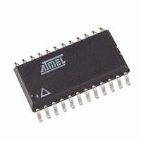
IC PLD 20NS OTP SO-24
Manufacturer
Atmel
Specifications of AT22LV10-20SI
Programmable Type
EPLD
Number Of Macrocells
10
Voltage - Input
3V
Speed
20ns
Mounting Type
Surface Mount
Package / Case
24-SOIC (7.5mm Width)
Family Name
AT22LV10
Process Technology
CMOS
# Macrocells
10
# I/os (max)
10
Frequency (max)
100MHz
Propagation Delay Time
20ns
Operating Supply Voltage (typ)
3.3/5V
Operating Supply Voltage (min)
3V
Operating Supply Voltage (max)
5.5V
Supply Current
45/100mA
Operating Temp Range
-40C to 85C
Operating Temperature Classification
Industrial
Mounting
Surface Mount
Pin Count
24
Package Type
SOIC
Lead Free Status / RoHS Status
Contains lead / RoHS non-compliant
Other names
AT22LV1020SI


Preload of Registered Outputs
The registers in the AT22LV10 and AT22LV10L are pro-
vided with circuitry to allow loading of each register
asynchronously with either a high or a low. This feature will
simplify testing since any state can be forced into the regis-
ters to control test sequencing. A V
will force the register high; a V
dent of the polarity bit (C0) setting. The preload state is
entered by placing an 11.5V to 13V signal on pin 8 on
Power-up Reset
The registers in the AT22LV10 and AT22LV10L are
designed to reset during power-up. At a point delayed
slightly from V
the low state. The output state will depend on the polarity of
the output buffer.
This feature is critical for state machine initialization.
However, due to the asynchronous nature of reset and the
uncertainty of how V
following conditions are required:
1. The V
2. After reset occurs, all input and feedback setup
3. The clock must remain stable during t
Pin Capacitance
(f = 1 MHz, T = 25°C)
Note:
Erasure Characteristics
The entire fuse array of an AT22LV10 or AT22LV10L is
erased after exposure to ultraviolet light at a wavelength of
2537 Å. Complete erasure is assured after a minimum of
20 minutes exposure using 12,000 µW/cm
spaced one inch away from the chip. Minimum erase time
for lamps at other intensity ratings can be calculated from
C
C
IN
OUT
times must be met before driving the clock pin high,
and
1. Typical values for nominal supply voltage. This parameter is only sampled and is not 100% tested.
CC
rise must be monotonis;
CC
crossing 2.5V, all registers will be reset to
(1)
CC
actually rises in the system, the
IL
will force it low, indepen-
IH
level on the I/O pin
Typ
5
6
PR
2
.
intensity lamps
Max
DIPs, and pin 10 on SMPs. When the clock pin is pulsed
high, the data on the I/O pins is placed into the ten
registers.
the minimum integrated erasure dose of 15 W
prevent unintentional erasure, an opaque label is recom-
mended to cover the clear window on any UV erasable
PLD which will be subjected to continuous fluorescent
indoor lighting or sunlight.
8
8
Level Forced on Registered Output
Parameter
t
PR
Pin During Preload Cycle
Power-up
Reset Time
Description
V
V
IH
IL
Units
pF
pF
AT22LV10(L)
Min
Conditions
V
V
IN
OUT
Typ
600
Register State After
= 0V
= 0V
Cycle
Max
1000
High
Low
•
sec/cm
Units
2
ns
. To
7
Related parts for AT22LV10-20SI
Image
Part Number
Description
Manufacturer
Datasheet
Request
R


Part Number:
Description:
At22lv10 Low-voltage Uv Erasable Programmable Logic Device
Manufacturer:
ATMEL Corporation
Datasheet:

Part Number:
Description:
IC PLD 20NS OTP 28PLCC
Manufacturer:
Atmel
Datasheet:
Part Number:
Description:
IC PLD 25NS OTP 28PLCC
Manufacturer:
Atmel
Datasheet:

Part Number:
Description:
Low-Voltage UV Erasable Programmable Logic Device
Manufacturer:
ATMEL [ATMEL Corporation]
Datasheet:

Part Number:
Description:
IC PLD 20NS OTP 24DIP
Manufacturer:
Atmel
Datasheet:
Part Number:
Description:
IC PLD 25NS OTP 24DIP
Manufacturer:
Atmel
Datasheet:

Part Number:
Description:
IC PLD EE 25NS LV UV 24-SOIC
Manufacturer:
Atmel
Datasheet:

Part Number:
Description:
DEV KIT FOR AVR/AVR32
Manufacturer:
Atmel
Datasheet: