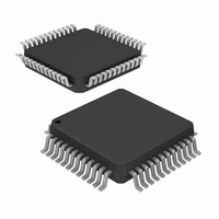
ISL5314INZ Intersil, ISL5314INZ Datasheet - Page 7

ISL5314INZ
Manufacturer Part Number
ISL5314INZ
Description
IC SYNTHESIZER DIGITAL 48-MQFP
Manufacturer
Intersil
Datasheet
1.ISL5314INZ.pdf
(17 pages)
Specifications of ISL5314INZ
Resolution (bits)
14 b
Master Fclk
125MHz
Tuning Word Width (bits)
48 b
Voltage - Supply
3 V ~ 5.5 V, 4.5 V ~ 5.5 V
Operating Temperature
-40°C ~ 85°C
Mounting Type
Surface Mount
Package / Case
48-LQFP
Supplier Package
LQFP
Resolution
14 Bit
Maximum Input Frequency
125(Min) MHz
Tuning Word Width
48 Bit
Minimum Operating Supply Voltage
4.5 V
Typical Operating Supply Voltage
5 V
Maximum Operating Supply Voltage
5.5 V
Minimum Operating Temperature
-40 °C
Maximum Operating Temperature
85 °C
Mounting
Surface Mount
Ic Function
Direct Digital Synthesizer
Supply Voltage Range
4.5V To 5.5V, 3V To 5.5V
Operating Temperature Range
-40°C To +85°C
Digital Ic Case Style
LQFP
No. Of Pins
48
Rohs Compliant
Yes
Lead Free Status / RoHS Status
Lead free / RoHS Compliant
Available stocks
Company
Part Number
Manufacturer
Quantity
Price
Company:
Part Number:
ISL5314INZ
Manufacturer:
PEREGRIN
Quantity:
2 800
where f
If M-ary FSK is required (more than two frequencies), the user
will have to continually reprogram the center frequency register.
The maximum write rate to the same parallel register is the
lesser of 50MSPS or f
every register updated. The maximum possible rate occurs if
the user only needs to change eight bits (one register). For
M-ary FSK, the output frequency rate of change is as shown in
Equation 7:
where REG = quantity of registers being written and
WR = write rate.
PSK Modulation
Binary or quadrature phase shift keying (PSK) can be done
by using the phase pins, PH0 and PH1. The change in
phase can be pipelined such that the PH pins can be toggled
at a rate up to as shown in Equation 8:
where f
Quadrature Local Oscillators
Two ISL5314s can be used as sine/cosine generators for
quadrature local oscillator applications. It is important to note
that the phase accumulator feedback needs to be zeroed in
both devices if it is desired that both DDSs restart with a
known phase, which is determined by the use of the phase
control pins, PH1 and PH0. To zero the phase accumulator,
pull Bit 5 of address 13 low and then high again at the same
time in both devices.
Squarewave Clock Source
The on-chip comparator can be used to generate a square
wave. The analog output is filtered and then fed into the
comparator input. Because the analog output is a sampled-
waveform, a high DAC output frequency (relative to the clock
rate) creates large amplitude steps in the sampled
waveform. These steps have to be smoothed with a lowpass
filter in order for the comparator to operate properly,
otherwise the zero-order hold nature of the sampled analog
output could possibly hold at the comparator’s trigger point
temporarily causing the comparator to toggle unexpectedly.
For this reason, it is very important that a lowpass filter be
used on the analog output prior to the input of the
comparator. The user can set one input to the comparator at
a DC reference point (typically the mid-point of the filtered
signal) and feed the filtered analog output into the other
input. See Figure 2 for an example of a square wave circuit
using this method. Since IOUTA and IOUTB are differential,
the mid-point between the 10k resistors will always be the
average value of each signal. The large resistors have to be
used so that the parallel resistance of the intended load and
the extra load of the averaging circuit yields a negligible
M-ary FSK Rate = WR/REG
PH
MAX
CLK
CLK
= f
CLK
is the frequency of the master CLK.
is the frequency of the master CLK.
/2
CLK
/2. One WR clock cycle is required for
7
(EQ. 7)
(EQ. 8)
ISL5314
effect on the intended load. The average value is used as
the reference voltage for one input to the comparator, with a
capacitor to filter off any high frequency noise. The other
comparator input is connected to the lowpass filter output. It
is important that both IOUTA and IOUTB are equally loaded
so that each generates the same amplitude and therefore
has the same average value.
The user can filter both IOUTA and IOUTB and feed them
differentially into the comparator. It is difficult to perfectly
match the differential option, so the single-ended option is
recommended. The jitter of the comparator is typically 500ps
peak to peak. The actual jitter achieved is partially
dependent on the quality of the signal at the comparator
input, which is dictated by the amount of oversampling of the
analog output and the quality of the lowpass filter.
The user also has the option to evaluate the comparator
circuit in Figure 2 with lower output current in order to save
power consumption in the ISL5314. The DAC output current
can be set to 5mA or 10mA instead of 20mA and evaluated
to determine if the comparator performance is still suitable
for the application. Since the output current is derived from
the +5V analog supply, reducing the output from 20mA to
10mA saves approximately 50mW of power. The
recommended minimum amplitude of the comparator input is
100mV, so operation of the analog outputs with less than
20mA of output current should be possible with appropriate
resistive loading (for example, 5mA into a 50Ω load provides
250mV of amplitude).
If needed, series resistance on the comparator output can be
used to reduce overshoot and/or ringing. The comparator
can be used to drive a 50Ω load.
ISL5314
PIN 22
PIN 23
PIN 18
PIN 17
PIN 10
FIGURE 2. SQUAREWAVE GENERATION USING THE
IN+
IN-
IOUTA
IOUTB
ON-CHIP COMPARATOR
COMPOUT
>1nF
COMPARATOR INPUTS
>10kΩ
>10kΩ
100Ω
50Ω
(TYP 20-40MHz)
LPF (100Ω)
100Ω
January 19, 2010
FN4901.3


