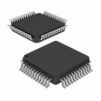
ISL5314IN Intersil, ISL5314IN Datasheet

ISL5314IN
Specifications of ISL5314IN
Available stocks
Related parts for ISL5314IN
ISL5314IN Summary of contents
Page 1
... UPDATE pin. Ordering Information PART PART TEMP. NUMBER MARKING RANGE (°C) ISL5314INZ ISL5314 INZ -40 to +85 ISL5314EVAL2 25 NOTES: 1. These Intersil Pb-free plastic packaged products employ special Pb-free material sets, molding compounds/die attach materials, and 100% matte tin plate plus anneal (e3 termination finish, which is RoHS compliant and compatible with both SnPb and Pb-free soldering operations) ...
Page 2
Pin Descriptions PIN NO. PIN NAME TYPE 44-48, 1-3 C(7:0) Input 42 WR Input 40 WE Input 35-38 A(3:0) Input 6 CLK Clock 8 RESET Input 30 SCLK Input 27 SDATA Input 32 SSYNC Input 9 UPDATE Input 33, 34 ...
Page 3
Typical Application Circuit (Parallel Control Mode, Sinewave Generation) µPROCESSOR/ 8 FPGA/CPLD CLOCK SOURCE f CLK DV P-P 0.1µF +5V POWER SOURCE 3 ISL5314 SDATA, SSYNC, SCLK (IN PARALLEL CONTROL MODE, SERIAL CONTROL CAN ALSO BE USED IF DESIRED.) WRITE CLOCK ...
Page 4
Functional Description The ISL5314 is an NCO with an integrated 14-bit DAC designed to run in excess of 125MSPS. The NCO is a 16-bit output design, which is rounded to fourteen bits for input to the DAC. The frequency control ...
Page 5
Bits 4444 4444 (Individual Bit Alignment) 7654 3210 Phase Accumulator xxxx xxxx Center Frequency xxxx xxxx Offset Frequency xxxx xxxx Serial Frequency, 8 Bits xxxx xxxx Serial Frequency, 16 Bits xxxx xxxx Serial Frequency, 24 Bits xxxx xxxx Serial ...
Page 6
I (Full Scale OUT FSADJ SET) Analog Output IOUTA and IOUTB are complementary current outputs. They are generated by a 14-bit DAC that is capable of running at the full 125MSPS rate. The DDS clock ...
Page 7
CLK. CLK If M-ary FSK is required (more than two frequencies), the user will have to continually reprogram the center frequency register. The maximum write rate to the same parallel register is ...
Page 8
... LQFP Package Maximum Junction Temperature . . . . . . . . . . . . . . . . . . . . . . +150°C + 0.3V Maximum Storage Temperature Range . . . . . . . . . .-65°C to +150° 0.3V Pb-Free Reflow Profile .see link below DD http://www.intersil.com/pbfree/Pb-FreeReflow.asp = DV = +5V (unless otherwise noted +25°C for All Typical Values. Boldface limits apply over the operating A TEST CONDITIONS , +5V AV ...
Page 9
Electrical Specifications AV DD all Min and Max Values. T temperature range, -40°C to +85°C. (Continued) PARAMETER Spurious Free Dynamic Range, f CLK SFDR to Nyquist (f /2) (Notes 7, 10) CLK f CLK f CLK f CLK f CLK ...
Page 10
Electrical Specifications AV DD all Min and Max Values. T temperature range, -40°C to +85°C. (Continued) PARAMETER Address Setup Time, t Between ADDR and WR (Note 6) AS Address Hold Time, t Between ADDR and WR (Note 6) AH UPDATE ...
Page 11
Electrical Specifications AV DD all Min and Max Values. T temperature range, -40°C to +85°C. (Continued) PARAMETER Input Resistance Input Current Maximum Input Voltage Allowed (Excluding Comparator Sleep Mode) Minimum Input Voltage, Peak-to-Peak (Dependent on Noise) Propagation Delay, High to ...
Page 12
Definition of Specifications Differential Non-Linearity (DNL) is the measure of the step size output deviation from code to code. Ideally the step size should be one LSB. A DNL specification of one LSB or less guarantees monotonicity. Integral Non-Linearity (INL) ...
Page 13
Timing Diagrams ADDR ADDR A 0 DATA WRITE CLK (f ) CLK UPDATE ANALOG OUT FIGURE 3. PARALLEL-LOAD METHOD 1, UPDATE ACTIVE AFTER LOADING REGISTERS (RESET = HIGH ...
Page 14
Timing Diagrams (Continued) ONE CLK RISING EDGE REQUIRED WHILE RESET LOW CLK (f ) CLK RESET ANALOG OUT CLK (f ) CLK ENOFR ANALOG OUT FIGURE 6. ENOFR (ENABLE OFFSET FREQUENCY REGISTER) TIMING AND LATENCY (RESET = HIGH) 14 ISL5314 ...
Page 15
Timing Diagrams (Continued) RESET t SDS SDATA SCLK t SSS SERIAL FREQ t REGISTER SSYNC t ) CLK (f CLK DON’T CARE (ASSUMED CONTINUOUSLY RUNNING) ANALOG OUT FIGURE 7. SERIAL PROGRAMMING, SYNC EARLY MODE (REPRESENTS MINIMUM SCLKS REQUIRED. SCLK CAN ...
Page 16
... This bit enables/disables the data path from the serial frequency register to the phase accumulator, without changing the value of the register. Should be disabled after RESET if not used. 5 Phase accumulator feedback accumulator feedback disabled accumulator enabled. 4:0 Intersil reserved. Do not change. 14 7:0 Test and timing control register. User must write 00h or 30h to register 14 after RESET. 5:4 NCO-to-DAC setup and hold timing control ...
Page 17
... Accordingly, the reader is cautioned to verify that data sheets are current before placing orders. Information furnished by Intersil is believed to be accurate and reliable. However, no responsibility is assumed by Intersil or its subsidiaries for its use; nor for any infringements of patents or other rights of third parties which may result from its use ...


