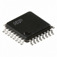
TDA8020HL/C2,118 NXP Semiconductors, TDA8020HL/C2,118 Datasheet - Page 15

TDA8020HL/C2,118
Manufacturer Part Number
TDA8020HL/C2,118
Description
IC SMART CARD INTERFACE 32LQFP
Manufacturer
NXP Semiconductors
Type
Interfacer
Datasheet
1.TDA8020HLC2118.pdf
(28 pages)
Specifications of TDA8020HL/C2,118
Package / Case
32-LQFP
Voltage - Supply
2.7 V ~ 6.5 V
Mounting Type
Surface Mount
Maximum Operating Temperature
+ 85 C
Minimum Operating Temperature
- 40 C
Mounting Style
SMD/SMT
Lead Free Status / RoHS Status
Lead free / RoHS Compliant
Number Of Drivers/receivers
-
Protocol
-
Lead Free Status / Rohs Status
Lead free / RoHS Compliant
Other names
568-3522-2
935272983118
TDA8020HL2BD-T
935272983118
TDA8020HL2BD-T
Available stocks
Company
Part Number
Manufacturer
Quantity
Price
Company:
Part Number:
TDA8020HL/C2,118
Manufacturer:
NXP Semiconductors
Quantity:
10 000
Part Number:
TDA8020HL/C2,118
Manufacturer:
NXP/恩智浦
Quantity:
20 000
Philips Semiconductors
Clock inputs and data inputs/outputs to the system controller
CLKIN1 is the input clock for card 1, CLKIN2 for card 2. They may be driven separately from the system controller, or be
tied together externally and driven by the same signal.
I/O1uC is the data signal to or from card 1, I/O2uC to or from card 2. They can be driven separately from the system
controller, in which case both bits I/OEN may be set to logic 1. They can also be driven by the same signal, which
requires them to be tied together externally, but each bit I/OEN has to be set or reset according to the addressed card.
LIMITING VALUES
In accordance with the Absolute Maximum Rating System (IEC 60134).
Notes
1. HBM: EIA/JESD22-A 114-B; June 2000.
2. All card contacts are protected against any short-circuit with any other card contact.
3. MM: EIA/JESD22-A 115-A; October 1997.
HANDLING
Inputs and outputs are protected against electrostatic discharge in normal handling. However it is good practice to take
normal precautions appropriate to handling MOS devices (see “Handling MOS devices” ).
THERMAL CHARACTERISTICS
2003 Nov 06
V
V
V
P
T
T
V
R
SYMBOL
SYMBOL
stg
j
DD
DDI
n
tot
esd
th(j-a)
Dual IC card interface
supply voltage on pins V
supply voltage for interface signals
input voltage
total power dissipation
storage temperature
junction temperature
electrostatic discharge voltage
thermal resistance from junction to ambient
on pins SAP, SAM, SBP, SBM and V
on pins SDA and SCL
on all other pins
PARAMETER
PARAMETER
DD
and V
DDA
UP
15
in free air
T
HMB; note 1
MM; note 3
amb
CONDITIONS
all card contact pins
within the typical
application; note 2
pins V
all other pins
all pins
= 40 C to +85 C
CONDITION
DDA
and V
DDI
VALUE
80
0.5
0.5
0.5
0.5
0.5
55
6
0.5
2
200
MIN.
TDA8020HL
Product specification
+6.5
+6.5
+7.5
+6.5
V
500
+150
125
+6
+2
0.5
200
DD
MAX.
+ 0.5
UNIT
K/W
V
V
V
V
V
mW
kV
kV
kV
V
UNIT
C
C


