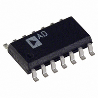
ADM489ARZ Analog Devices Inc, ADM489ARZ Datasheet - Page 6

ADM489ARZ
Manufacturer Part Number
ADM489ARZ
Description
IC TX/RX RS485 LO-SLEW/EN 14SOIC
Manufacturer
Analog Devices Inc
Type
Transceiverr
Datasheet
1.ADM489ARZ.pdf
(16 pages)
Specifications of ADM489ARZ
Number Of Drivers/receivers
1/1
Protocol
RS422, RS485
Voltage - Supply
4.5 V ~ 5.5 V
Mounting Type
Surface Mount
Package / Case
14-SOIC (3.9mm Width), 14-SOL
Device Type
Differential Line Transceiver
Ic Interface Type
RS485
No. Of Drivers
1
Supply Voltage Range
4.5V To 5.5V
Driver Case Style
SOIC
No. Of Pins
14
Lead Free Status / RoHS Status
Lead free / RoHS Compliant
Available stocks
Company
Part Number
Manufacturer
Quantity
Price
Company:
Part Number:
ADM489ARZ
Manufacturer:
ADI
Quantity:
296
Part Number:
ADM489ARZ
Manufacturer:
ADI/亚德诺
Quantity:
20 000
Part Number:
ADM489ARZ-REEL7
Manufacturer:
ADI/亚德诺
Quantity:
20 000
ADM488/ADM489
PIN CONFIGURATIONS AND FUNCTION DESCRIPTIONS
Table 4. ADM488 Pin Function Descriptions
Pin No.
1
2
3
4
5
6
7
8
Table 5. ADM489 Pin Function Descriptions
PDIP/SOIC
Pin No.
1, 8, 13
2
3
4
5
6, 7
9
10
11
12
14
Figure 4. ADM489 14-Lead PDIP/SOIC Pin Configuration
V
RO
DI
GND
Y
Z
B
A
Mnemonic
CC
TSSOP
Pin No.
2, 9, 10, 13,
16
3
4
5
6
7, 8
11
12
14
15
1
GND
GND
RO
NC
RE
DE
DI
1
2
3
4
5
6
7
NC = NO CONNECT
(Not to Scale)
ADM489
TOP VIEW
Description
Power Supply, 5 V ± 10%.
Receiver Output. When A > B by 200 mV, RO = high. If A < B by 200 mV, RO = low.
Driver Input. A logic low on DI forces Y low and Z high, while a logic high on DI forces Y high and Z low.
Ground Connection, 0 V.
Inverting Driver, Output Z.
Inverting Receiver, Input B.
Noninverting Receiver, Input A.
Noninverting Driver, Output Y.
Mnemonic
NC
RO
RE
DE
DI
GND
Y
Z
B
A
V
CC
14
13
12
11
10
9
8
V
NC
A
B
Z
Y
NC
CC
Description
No Connect. No connections are required to this pin.
Receiver Output. When enabled, if A > B by 200 mV then RO = high. If A < B by 200 mV then
RO = low.
Receiver Output Enable. A low level enables the receiver output, RO. A high level places it in a
high impedance state.
Driver Output Enable. A high level enables the driver differential outputs, Y and Z. A low level
places it in a high impedance state.
Driver Input. When the driver is enabled, a logic low on DI forces Y low and Z high, while a logic
high on DI forces Y high and Z low.
Ground Connection, 0 V.
Noninverting Driver, Output Y.
Inverting Driver, Output Z.
Inverting Receiver, Input B.
Noninverting Receiver, Input A.
Power Supply, 5 V ± 10%.
Figure 3. ADM488 8-Lead PDIP/SOIC Pin Configuration
GND
V
RO
CC
DI
Rev. D | Page 6 of 16
1
2
3
4
(Not to Scale)
ADM488
TOP VIEW
8
7
6
5
A
B
Z
Y
Figure 5. ADM489 16-Lead TSSOP Pin Configuration
GND
GND
V
RO
NC
RE
DE
CC
DI
1
2
3
4
5
6
7
8
NC = NO CONNECT
(Not to Scale)
ADM489
TOP VIEW
15
14
13
12
11
10
16
9
NC
A
B
NC
Z
Y
NC
NC


