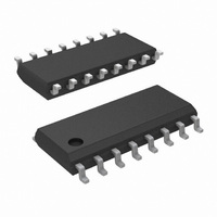
DS90LV031ATM/NOPB National Semiconductor, DS90LV031ATM/NOPB Datasheet

DS90LV031ATM/NOPB
Specifications of DS90LV031ATM/NOPB
*DS90LV031ATM/NOPB
DS90LV031ATM
Available stocks
Related parts for DS90LV031ATM/NOPB
DS90LV031ATM/NOPB Summary of contents
Page 1
... Order Number DS90LV031ATM or DS90LV031ATMTC See NS Package Number M16A or MTC16 Truth Table All other combinations of ENABLE inputs TRI-STATE ® registered trademark of National Semiconductor Corporation. © 2010 National Semiconductor Corporation DS90LV031A Features ■ >400 Mbps (200 MHz) switching rates ■ 0.1 ns typical differential skew ■ ...
Page 2
... Absolute Maximum Ratings If Military/Aerospace specified devices are required, please contact the National Semiconductor Sales Office/ Distributors for availability and specifications. Supply Voltage ( Input Voltage ( Enable Input Voltage (EN, EN*) Output Voltage ( OUT+ OUT− Short Circuit Duration ( OUT+ OUT− Maximum Package Power Dissipation @ +25°C ...
Page 3
Switching Characteristics - Industrial V = +3.3V ±10 −40°C to +85° Symbol Parameter t Differential Propagation Delay High to Low PHLD t Differential Propagation Delay Low to High PLHD t Differential Pulse Skew |t SKD1 PHLD ...
Page 4
Parameter Measurement Information FIGURE 2. Driver Propagation Delay and Transition Time Test Circuit FIGURE 3. Driver Propagation Delay and Transition Time Waveforms www.national.com FIGURE 1. Driver V and V Test Circuit 10009503 10009504 10009505 ...
Page 5
FIGURE 4. Driver TRI-STATE Delay Test Circuit FIGURE 5. Driver TRI-STATE Delay Waveform 5 10009506 10009507 www.national.com ...
Page 6
Applications Information General application guidelines and hints for LVDS drivers and receivers may be found in the following application notes: LVDS Owner's Manual (lit #550062-001), AN808, AN1035, AN977, AN971, AN916, AN805, AN903. LVDS drivers and receivers are intended to be ...
Page 7
Probing LVDS Transmission Lines: Always use high impedance (> 100kΩ), low capacitance (< 2pF) scope probes with a wide bandwidth (1GHz) scope. Improper probing will give deceiving results. Cables and Connectors, General Comments: When choosing cable and connectors for LVDS ...
Page 8
Typical Performance Curves FIGURE 8. Typical DS90LV031A, D Pin Descriptions Pin Ordering Information Package Type SOP TSSOP www.national.com (single ended OUT ...
Page 9
Physical Dimensions inches (millimeters) unless otherwise noted 16-Lead (0.150 Wide) Molded Small Outline Package, JEDEC 16-Lead (0.100 Wide) Molded Thin Shrink Small Outline Package, JEDEC Order Number DS90LV031ATM NS Package Number M16A Order Number DS90LV031ATMTC NS Package Number MTC16 9 ...
Page 10
... For more National Semiconductor product information and proven design tools, visit the following Web sites at: www.national.com Products Amplifiers www.national.com/amplifiers Audio www.national.com/audio Clock and Timing www.national.com/timing Data Converters www.national.com/adc Interface www.national.com/interface LVDS www.national.com/lvds Power Management www.national.com/power Switching Regulators www.national.com/switchers LDOs www.national.com/ldo LED Lighting www ...


