DP83849CVS/NOPB National Semiconductor, DP83849CVS/NOPB Datasheet - Page 39
DP83849CVS/NOPB
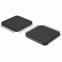
Manufacturer Part Number
DP83849CVS/NOPB
Description
IC TXRX ETHERNET PHY DUAL 80TQFP
Manufacturer
National Semiconductor
Type
Transceiverr
Specifications of DP83849CVS/NOPB
Number Of Drivers/receivers
2/2
Protocol
Ethernet
Voltage - Supply
3 V ~ 3.6 V
Mounting Type
Surface Mount
Package / Case
80-TQFP, 80-VQFP
Data Rate
100Mbps
Supply Voltage Range
3V To 3.6V
Logic Case Style
TQFP
No. Of Pins
80
Operating Temperature Range
0°C To +70°C
Msl
MSL 3 - 168 Hours
Filter Terminals
SMD
Rohs Compliant
Yes
Data Rate Max
10Mbps
For Use With
DP83849CVS-EVK - BOARD EVALUATION DP83849CVS
Lead Free Status / RoHS Status
Lead free / RoHS Compliant
Other names
*DP83849CVS
*DP83849CVS/NOPB
DP83849CVS
*DP83849CVS/NOPB
DP83849CVS
Available stocks
Company
Part Number
Manufacturer
Quantity
Price
Company:

Part Number:
DP83849CVS/NOPB
Manufacturer:
NS
Quantity:
618
Company:
Part Number:
DP83849CVS/NOPB
Manufacturer:
Texas Instruments
Quantity:
10 000


5.7.1.3 100MB Cable Length Estimation
The DP83849C provides a method of estimating cable
length based on electrical characteristics of the 100Mb
Link. This essentially provides an effective cable length
rather than a measurement of the physical cable length.
The cable length estimation is only available in 100Mb
mode of operation with a valid Link status. The cable
length estimation is available at the Link Diagnostics Reg-
isters
(LEN100_DET), address 14h.
5.7.1.4 Frequency Offset Relative to Link Partner
As part of the 100Mb clock recovery process, the DSP
implementation provides a frequency control parameter.
This value may be used to indicate the frequency offset of
the device relative to the link partner. This operation is only
available in 100Mb operation with a valid link status. The
frequency offset can be determined using the register
100Mb Frequency Offset Indication (FREQ100), address
15h, of the Link Diagnostics Registers - Page 2.
Two different versions of the Frequency Offset may be
monitored through bits [7:0] of register FREQ100 (15h).
The first is the long-term Frequency Offset. The second is
the current Frequency Control value, which includes short-
term phase adjustments and can provide information on
the amount of jitter in the system.
5.7.1.5 Cable Signal Quality Estimation
The cable signal quality estimator keeps a simple tracking
of results of the DSP and can be used to generate an
approximate Signal-to-Noise Ratio for the 100Mb receiver.
This information is available to software through the Link
Diagnostics Registers - Page 2: Variance Control
(VAR_CTRL), address 1Ah and Data (VAR_DATA),
address 1Bh.
The variance computation times (VAR_TIMER) can be
chosen from the set of {2, 4, 6, 8} ms. The 32-bit variance
sum can be read by two consecutive reads of the
VAR_DATA register. This sum can be used to compute an
SNR estimate by software using the following equation:
SNR = 10log10((37748736 * VAR_TIMER) / Variance).
5.7.2 Link Quality Monitor
The Link Quality Monitor allows a method to generate an
alarm when the DSP adaption strays from a programmable
window. This could occur due to changes in the cable
which could indicate a potential problem. Software can
program thresholds for the following DSP parameters to be
used to interrupt the system:
— Digital Equalizer C1 Coefficient (DEQ C1)
— Digital Adaptive Gain Control (DAGC)
— Digital Base-Line Wander Control (DBLW)
— Recovered Clock Long-Term Frequency Offset (FREQ)
— Recovered Clock Frequency Control (FC)
-
Page
2,
register
100Mb
Length
Detect
39
Software is expected to read initial adapted values and
then program the thresholds based on an expected valid
range. This mechanism takes advantage of the fact that
the DSP adaption should remain in a relatively small range
once a valid link has been established.
5.7.2.1 Link Quality Monitor Control and Status
Control of the Link Quality Monitor is done through the Link
Quality Monitor Register (LQMR), address 1Dh and the
Link Quality Data Register (LQDR), address 1Bh of the
Link Diagnostics Registers - Page 2. The LQMR register
includes a global enable to enable the Link Quality Monitor
function. In addition, it provides warning status from both
high and low thresholds for each of the monitored parame-
ters. Note that individual low or high parameter threshold
comparisons can be disabled by setting to the minimum or
maximum values.
To allow the Link Quality Monitor to interrupt the system,
the Interrupt must be enabled through the interrupt control
registers, MICR (11h) and MISR (12h).
5.7.2.2 Checking Current Parameter Values
Prior to setting Threshold values, it is recommended that
software check current adapted values. The thresholds
may then be set relative to the adapted values. The current
adapted values can be read using the LQDR register by
setting the Sample_Param bit [13] of LQDR, address
(1Eh).
For example, to read the DBLW current value:
5.7.2.3 Threshold Control
The LQDR (1Eh) register also provides a method of pro-
gramming high and low thresholds for each of the four
parameters that can be monitored. The register imple-
ments an indirect read/write mechanism.
Writes are accomplished by writing data, address, and a
write strobe to the register. Reads are accomplished by
writing the address to the register, and reading back the
value of the selected threshold. Setting thresholds to the
maximum or minimum values will disable the threshold
comparison since values have to exceed the threshold to
generate a warning condition.
Warnings are not generated if the parameter is equal to the
threshold. By default, all thresholds are disabled by setting
to the min or max values. The following table shows the
four parameters and range of values:
1. Write 2400h to LQDR (1Eh) to set the Sample_Param
2. Read LQDR (1Eh). Current DBLW value is returned
bit and set the LQ_PARAM_SEL[2:0] to 010.
in the low 8 bits.
www.national.com
Related parts for DP83849CVS/NOPB
Image
Part Number
Description
Manufacturer
Datasheet
Request
R

Part Number:
Description:
National Semiconductor [8-Bit D/A Converter]
Manufacturer:
National Semiconductor
Datasheet:
Part Number:
Description:
National Semiconductor [Media Coprocessor]
Manufacturer:
National Semiconductor
Datasheet:
Part Number:
Description:
Digitally Controlled Tone and Volume Circuit with Stereo Audio Power Amplifier, Microphone Preamp Stage and National 3D Sound
Manufacturer:
National Semiconductor
Datasheet:
Part Number:
Description:
Digitally Controlled Tone and Volume Circuit with Stereo Audio Power Amplifier, Microphone Preamp Stage and National 3D Sound
Manufacturer:
National Semiconductor
Datasheet:
Part Number:
Description:
AC97 Rev 2 Codec with Sample Rate Conversion and National 3D Sound
Manufacturer:
National Semiconductor
Part Number:
Description:
Manufacturer:
National Semiconductor
Datasheet:
Part Number:
Description:
Manufacturer:
National Semiconductor
Datasheet:
Part Number:
Description:
General Purpose, Low Voltage, Low Power, Rail-to-Rail Output Operational Amplifiers
Manufacturer:
National Semiconductor
Datasheet:
Part Number:
Description:
8-bit 20 MSPS flash A/D converter.
Manufacturer:
National Semiconductor
Datasheet:
Part Number:
Description:
Low Noise Quad Operational Amplifier
Manufacturer:
National Semiconductor
Datasheet:
Part Number:
Description:
Quad Differential Line Receivers
Manufacturer:
National Semiconductor
Datasheet:
Part Number:
Description:
Quad High Speed Trapezoidal? Bus Transceiver
Manufacturer:
National Semiconductor
Datasheet:
Part Number:
Description:
Dual Line Receiver
Manufacturer:
National Semiconductor
Datasheet:
Part Number:
Description:
TTL to 10k ECL Level Translator with Latch
Manufacturer:
National Semiconductor
Datasheet: