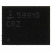
ISL59910IRZ Intersil, ISL59910IRZ Datasheet - Page 10

ISL59910IRZ
Manufacturer Part Number
ISL59910IRZ
Description
IC RCVR/EQUALZR TRPL DIFF 28-QFN
Manufacturer
Intersil
Type
Receiverr
Datasheet
1.ISL59910IRZ.pdf
(12 pages)
Specifications of ISL59910IRZ
Number Of Drivers/receivers
0/3
Protocol
Twisted-Pair
Voltage - Supply
5V
Mounting Type
Surface Mount
Package / Case
24-VQFN Exposed Pad, 24-HVQFN, 24-SQFN, 24-DHVQFN
Lead Free Status / RoHS Status
Lead free / RoHS Compliant
Available stocks
Company
Part Number
Manufacturer
Quantity
Price
Company:
Part Number:
ISL59910IRZ
Manufacturer:
Intersil
Quantity:
78
Company:
Part Number:
ISL59910IRZ
Manufacturer:
Nuvoton
Quantity:
482
Part Number:
ISL59910IRZ
Manufacturer:
INTERSIL
Quantity:
20 000
Company:
Part Number:
ISL59910IRZ-T7
Manufacturer:
INTERSIL
Quantity:
1 000
Part Number:
ISL59910IRZ-T7
Manufacturer:
INTERSIL
Quantity:
20 000
Contrast
By varying the voltage between pins VGAIN and VREF, the
gain of the signal path can be changed in the ratio 4:1. The
gain change varies almost linearly with control voltage. For
normal operation it is anticipated the X2 mode will be selected
and the output load will be back matched. A unity gain to the
output load will then be achieved with a gain control voltage of
about 0.35V. This allows the gain to be trimmed up or down by
6dB to compensate for any gain/loss errors that affect the
contrast of the video signal. Figure 26 shows an example plot
of the gain to the load with gain control voltage.
C
The ISL59910 features common mode decoding to allow
horizontal and vertical synchronization information, which has
been encoded on the three differential inputs by the EL4543,
to be decoded. The entire RGB video signal can therefore be
transmitted, along with the associated synchronization
information, by using just three twisted pairs.
Decoding is based on the EL4543 encoding scheme, as
described in Figure 26 and Table 1. The scheme is a three-level
system, which has been designed such that the sum of the
common mode voltages results in a fixed average DC level with
no AC content. This eliminates the effect of EMI radiation into
the common mode signals along the twisted pairs of the cable
The common mode voltages are initially extracted by the
ISL59910 from the three input pairs. These are then passed to
ommon Mode Sync Decoding
FIGURE 25. VARIATION OF GAIN WITH GAIN CONTROL
1.8
1.6
1.4
1.2
0.8
0.6
0.4
2
1
0
VOLTAGE
0.2
0.4
10
V
GAIN
0.6
0.8
1
ISL59910, ISL59913
an internal logic decoding block to provide Horizontal and
Vertical sync output signals (H
NOTE: Level ‘Mid’ is halfway between ‘High’ and ‘Low’
Power Dissipation
The ISL59910 and ISL59913 are designed to operate with
±5V supply voltages. The supply currents are tested in
production and guaranteed to be less than 39mA per
channel. Operating at ±5V power supply, the total power
dissipation is:
where:
• PD
• V
• I
• V
R
θ
calculated. This is done using Equation 3:
PD
PD
JA
L
channel = 39mA
application = 2V
RED CM
MAX
MAX
MAX
= Load resistance = 150Ω
S
OUTMAX
required for long term reliable operation can be
High
Low
Mid
Mid
MAX
= Supply voltage = 5V
= Maximum quiescent supply current per
=
=
1.29W
3
= Maximum power dissipation
FIGURE 26. H AND V SYNCS ENCODED
×
TABLE 1. H AND V SYNC DECODING
= Maximum output voltage swing of the
GREEN CM
2
×
High
High
Low
Low
V
S
×
TIME (0.5ms/DIV)
I
SMAX
BLUE CM
OUT
+
High
Low
Mid
Mid
Ω
(
V
S
and V
- V
OUTMAX
OUT
H
High
High
SYNC
Low
Low
).
)
December 15, 2006
×
V
--------------------------- -
BLUE CM
OUT (CH A)
GREEN CM
OUT (CH B)
RED CM
OUT (CH C)
V
H
OUTMAX
SYNC
V
SYNC
High
High
R
SYNC
Low
Low
(EQ. 1)
FN6406.0
(EQ. 2)
L


