DS2148T+ Maxim Integrated Products, DS2148T+ Datasheet
DS2148T+
Specifications of DS2148T+


Related parts for DS2148T+

DS2148T+ Summary of contents
Page 1
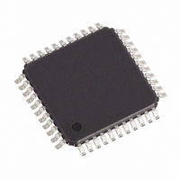
... E1/T1/J1 Line Interface Unit PIN CONFIGURATION TOP VIEW 1 See Section 8 for 144-pin CSBGA pinout. ORDERING INFORMATION PART CHANNEL DS2148TN Single DS2148TN+ Single DS2148T Single DS2148T+ Single DS2148GN Single DS2148GN Single DS2148G Single DS2148G+ Single DS21Q48N Four DS21Q48 Four + Denotes lead-free/RoHS-compliant package ...
Page 2
DETAILED DESCRIPTION .................................................................................................. 5 1 UNCTION ESCRIPTION 1 OCUMENT EVISION 2 PIN DESCRIPTION............................................................................................................ 10 3 HARDWARE MODE .......................................................................................................... 23 3 .............................................................................................................................23 EGISTER AP 3 ARALLEL ORT PERATION 3 ...
Page 3
Figure 1-1. DS2148 Block Diagram ............................................................................................................7 Figure 1-2. Receive Logic...........................................................................................................................8 Figure 1-3. Transmit Logic..........................................................................................................................9 Figure 2-1. Parallel Port Mode Pinout (BIS1 = 0, BIS0 = (TQFP Package) ..................................21 Figure 2-2. Serial Port Mode Pinout (BIS1 = 1, ...
Page 4
Table 2-1. Bus Interface Selection ...........................................................................................................10 Table 2-2. Pin Assignment in Parallel Port Mode .....................................................................................10 Table 2-3. Pin Descriptions in Parallel Port Mode (Sorted by Pin Name, DS2148T) ...............................12 Table 2-4. Pin Assignment in Serial Port Mode ........................................................................................14 Table 2-5. ...
Page 5
DETAILED DESCRIPTION The DS2148 is a complete selectable Line Interface Unit (LIU) for short- and long-haul applications. Throughout the data sheet represented wherever T1 exists. Receive sensitivity adjusts automatically to the incoming signal and ...
Page 6
Document Revision History 1) 100Ω/60Ω termination reversed in Internal Rx Termination Select tables, 091799. 2) Add DS21Q48 pinout, 092899. 3) Correct VSM pin number in Q48 ( BGA) from G5 to G4, 120699. 4) Add timing diagram ...
Page 7
Figure 1-1. DS2148 Block Diagram Unframed All Ones Insertion JACLK Jitter Attenuator MUX 2.048MHz to 1.544MHz PLL 16.384MHz or 8.192MHz or 4.096MHz or 2.048MHz BPCLK Synthesizer RPOS See Figure 3-2 RCLK RNEG PBEO MUX RCL/LOTC TPOS TCLK ...
Page 8
Figure 1-2. Receive Logic Clock Invert From Routed to Remote All Blocks CCR2.0 Loopback CCR2 Zero Detect 16 Zero Detect RIR1.7 RIR1.6 NRZ Data B8ZS/HDB3 Decoder BPV/CV/EXZ All Ones Loop Code Detector Detector CCR6.2/ RIR1.5 CCR6.0/ CCR6.1 ...
Page 9
Figure 1-3. Transmit Logic CCR1.6 OR Gate CCR3.1 1 BPV mux To Insert Remote Loopback 0 Routed to All Blocks CCR2.2 CCR3.0 B8ZS/ Logic HDB3 Error Coder Insert 0 0 mux 1 mux OR Gate RCLK 1 AND CCR1.1 Gate ...
Page 10
PIN DESCRIPTION The DS2148 can be controlled in a parallel port mode, a serial port mode hardware mode Table 2-2, and Table 2-3). The parallel and serial port modes are described in Section hardware mode is described ...
Page 11
DS2148T DS2148G PIN # PIN PARALLEL I/O PORT ...
Page 12
Table 2-3. Pin Descriptions in Parallel Port Mode (Sorted by Pin Name, DS2148T) NAME PIN I ALE(AS) 4 BIS0/BIS1 32/33 BPCLK D0/AD0 I/O D7/AD7 12 HRST 29 INT ...
Page 13
NAME PIN I/O RNEG 39 O RPOS 38 O RTIP/RRING 27/28 TCLK 43 TEST 26 TNEG 42 TPOS 41 TTIP/TRING 34/ 21/36 DD VSM 20 V 22/ (R/W) Receive Negative Data. Updated on the rising ...
Page 14
Table 2-4. Pin Assignment in Serial Port Mode DS2148T DS2148G PIN # PIN ...
Page 15
Table 2-5. Pin Descriptions in Serial Port Mode (Sorted by Pin Name, DS2148T) NAME PIN I/O BIS0/BIS1 32/33 BPCLK HRST 29 ICES 8 INT 23 MCLK OCES 9 PBEO 24 RCLK 40 RCL/LOTC 25 ...
Page 16
NAME PIN I/O SDI 6 I SDO 7 O TCLK 43 I TEST 26 I TNEG 42 I TPOS 41 I TTIP/TRING 34/ 21/ VSM 22/ FUNCTION Serial Data Input. Sampled ...
Page 17
Table 2-6. Pin Assignment in Hardware Mode DS2148T DS2148G PIN # PIN ...
Page 18
Table 2-7. Pin Description in Hardware Mode (Sorted by Pin Name, DS2148T) NAME PIN I/O BIS0/BIS1 32/33 I BPCLK 31 O CES 12 I DJA 8 I EGL 1 I ETS 2 I HBE 11 I HRST 29 I JAMUX ...
Page 19
NAME PIN I/O NRZE 3 I PBEO 24 O RCLK 40 O RCL 25 O RNEG 39 O RPOS 38 O RT0/RT1 44/23 I RTIP/ 27/28 I RRING SCLKE 4 I TCLK 43 I TEST 26 I TNEG 42 I ...
Page 20
Table 2-8. Loopback Control in Hardware Mode LOOPBACK SYMBOL Remote Loopback Local Loopback Analog Loopback No Loopback Table 2-9. Transmit Data Control in Hardware Mode TRANSMIT DATA Transmit Unframed All Ones Transmit Alternating Ones and Zeros Transmit PRBS TPOS and ...
Page 21
Figure 2-1. Parallel Port Mode Pinout (BIS1 = 0, BIS0 = (TQFP Package (DS) 3 WR* (R/W*) 4 ALE (AS ...
Page 22
Figure 2-3. Hardware Mode Pinout (BIS1 = 1, BIS0 = 1) (TQFP Package NRZE 4 SCLKE DJA 9 JAM UX 10 JAS 11 HBE BIS1 33 ...
Page 23
HARDWARE MODE In hardware mode (BIS1 = 1, BIS0 = 1), pins 1-19, 23, 25, 31, and 44 are redefined to be used for initializing the DS2148. BPCLK (pin 31) defaults to a 16.384MHz output when in hardware mode. ...
Page 24
Parallel Port Operation When using the parallel interface on the DS2148 (BIS1 = 0) the user has the option for either multiplexed bus operation (BIS1 = 0, BIS0 = 0) or nonmultiplexed bus operation (BIS1 = 0, BIS0 = ...
Page 25
Figure 3-1. Serial Port Operation for Read Access ( Mode 1 ICES = 1 (sample SDI on the falling edge of SCLK) OCES = 1 (update SDO on rising edge of SCLK) SCLK ...
Page 26
Figure 3-3. Serial Port Operation for Read Access Mode 3 ICES = 0 (sample SDI on the rising edge of SCLK) OCES = 0 (update SDO on falling edge of SCLK) SCLK SDI A0 A1 ...
Page 27
Figure 3-5. Serial Port Operation for Write Access ( Modes 1 and 2 ICES = 1 (sample SDI on the falling edge of SCLK) SCLK SDI (lsb) ...
Page 28
CONTROL REGISTERS CCR1 (00H): COMMON CONTROL REGISTER 1 (MSB) ETS NRZE RCLA SYMBOL POSITION ETS CCR1.7 NRZE CCR1.6 RCLA CCR1.5 ECUE CCR1.4 JAMUX CCR1.3 TTOJ CCR1.2 TTOR CCR1.1 LOTCMC CCR1.0 ECUE JAMUX TTOJ DESCRIPTION E1/T1 Select ...
Page 29
Table 4-1. MCLK Selection JAMUX MCLK (CCR1.3) 2.048MHz 0 2.048MHz 1 1.544MHz 0 CCR2 (01H): COMMON CONTROL REGISTER 2 (MSB) P25S N/A SYMBOL POSITION P25S CCR2.7 - CCR2.6 SCLD CCR2.5 CLDS CCR2.4 RHBE CCR2.3 THBE CCR2.2 TCES CCR2.1 RCES CCR2.0 ...
Page 30
CCR3 (02H): COMMON CONTROL REGISTER 3 (MSB) TUA1 ATUA1 TAOZ SYMBOL POSITION TUA1 CCR3.7 ATUA1 CCR3.6 TAOZ CCR3.5 TPRBSE CCR3.4 TLCE CCR3.3 LIRST CCR3.2 IBPV CCR3.1 IBE CCR3.0 TPRBSE TLCE DESCRIPTION Transmit Unframed All Ones. The polarity of this bit ...
Page 31
Device Power-Up and Reset The DS2148 will reset itself upon power-up, setting all writeable registers to 00h and clearing the status and information registers. CCR3.7 (TUA1 results in the LIU transmitting unframed all ones. After the power ...
Page 32
CCR5 (04H): COMMON CONTROL REGISTER 5 (MSB) BPCS1 BPCS0 SYMBOL POSITION BPCS1 CCR5.7 BPCS0 CCR5.6 MM1 CCR5.5 MM0 CCR5.4 RSCLKE CCR5.3 TSCLKE CCR5.2 RT1 CCR5.1 RT0 CCR5.0 Table 4-3. Backplane Clock Select BPCS1 BPCS0 (CCR5.7) (CCR5. ...
Page 33
Table 4-5. Internal Rx Termination Select RT1 RT0 (CCR5.1) (CCR5. CCR6 (05H): COMMON CONTROL REGISTER 6 (MSB) LLB RLB ARLBE SYMBOL POSITION LLB CCR6.7 RLB CCR6.6 ARLBE CCR6.5 ALB CCR6.4 INTERNAL RECEIVE ...
Page 34
SYMBOL POSITION RJAB CCR6.3 ECRS2 CCR6.2 ECRS1 CCR6.1 ECRS0 CCR6.0 5 STATUS REGISTERS There are three registers that contain information on the current real-time status of the device, status register (SR), and receive information registers 1 and 2 (RIR1/RIR2). When ...
Page 35
Table 5-1. Received Alarm Criteria ALARM E1/T1 RUA1 E1 RUA1 T1 1 RCL E1 1 RCL T1 NOTES: 1) Receive carrier loss (RCL) is also known as loss-of-signal (LOS) or Red Alarm in T1. 2) See CCR1.5 for details. SR ...
Page 36
IMR (07H): INTERRUPT MASK REGISTER (MSB) LUP LDN LOTC SYMBOL POSITION LUP IMR.7 LDN IMR.6 LOTC IMR.5 RUA1 IMR.4 RCL IMR.3 TCLE IMR.2 TOCD IMR.1 PRBSD IMR.0 RUA1 RCL TCLE DESCRIPTION Loop Up Code Detected interrupt masked 1 ...
Page 37
RIR1 (08H): RECEIVE INFORMATION REGISTER 1 (MSB) ZD 16ZD SYMBOL POSITION ZD RIR1.7 (latched) 16ZD RIR1.6 (latched) HBD RIR1.5 (latched) RCLC RIR1.4 (latched) RUA1C RIR1.3 (latched) JALT RIR1.2 (latched) N/A RIR1.1 N/A RIR1.0 HBD RCLC RUA1C DESCRIPTION Zero Detect. Set ...
Page 38
RIR2 (09H): RECEIVE INFORMATION REGISTER 2 (MSB) RL3 RL2 SYMBOL POSITION RL3 RIR2.7 (real time) RL2 RIR2.6 (real time) RL1 RIR2.5 (real time) RL0 RIR2.4 (real time) N/A RIR2.3 N/A RIR2.2 ARLB RIR2.1 (real time) SEC RIR2.0 (latched) Table 5-2. ...
Page 39
DIAGNOSTICS 6.1 In-Band Loop Code Generation and Detection The DS2148 can generate and detect a repeating bit pattern that is from one to eight or sixteen bits in length. To transmit a pattern, the user will load the pattern ...
Page 40
Table 6-1. Transmit Code Length LENGTH SELECTED TC1 TC0 (BITS 6 16/8/4/2/1 Table 6-2. Receive Code Length RUP2/RDN2 RUP1/RDN1 ...
Page 41
TCD2 (0CH): TRANSMIT CODE DEFINITION REGISTER 2 (MSB) C15 C14 SYMBOL POSITION C15 TCD2.7 C14 TCD2.6 C13 TCD2.5 C12 TCD2.4 C11 TCD2.3 C10 TCD2.2 C9 TCD2.1 C8 TCD2.0 RUPCD1 (0DH): RECEIVE UP CODE DEFINITION REGISTER 1 (MSB SYMBOL ...
Page 42
RUPCD2 (0EH): RECEIVE UP CODE DEFINITION REGISTER 2 (MSB) C15 C14 SYMBOL POSITION C15 RUPCD2.7 C14 RUPCD2.6 C13 RUPCD2.5 C12 RUPCD2.4 C11 RUPCD2.3 C10 RUPCD2.2 C9 RUPCD2.1 C8 RUPCD2.0 RDNCD1 (0FH): RECEIVE DOWN CODE DEFINITION REGISTER 1 (MSB ...
Page 43
RDNCD2 (10H): RECEIVE DOWN CODE DEFINITION REGISTER 2 (MSB) C15 C14 SYMBOL POSITION C15 RDNCD2.7 C14 RDNCD2.6 C13 RDNCD2.5 C12 RDNCD2.4 C11 RDNCD2.3 C10 RDNCD2.2 C9 RDNCD2.1 C8 RDNCD2.0 6.2 Loopbacks 6.2.1 Remote Loopback (RLB) When RLB (CCR6.6) is enabled, ...
Page 44
Analog Loopback (ALB) Setting ALB (CCR6. one puts the DS2148 in Analog Loopback. Signals at TTIP and TRING will be internally connected to RTIP and RRING. The incoming signals at RTIP and RRING will be ignored. The ...
Page 45
Table 6-4. Function of ECRS Bits and RNEG Pin ECRS2 ECRS1 (CCR1.7) (CCR6.2) (CCR6. NOTES: 1) RNEG outputs error ...
Page 46
ANALOG INTERFACE 7.1 Receiver The DS2148 contains a digital clock recovery system. The DS2148 couples to the receive twisted pair (or coaxial cable in 75Ω E1 applications) via a 1:1 transformer. See details. Figure 7-1, Figure ...
Page 47
Transmitter The DS2148 uses a set of laser-trimmed delay lines along with a precision digital-to-analog converter (DAC) to create the waveforms that are transmitted onto the line. The waveforms created by the DS2148 meet the latest ...
Page 48
G.703 Synchronization Signal The DS2148 is capable of receiving a 2.048MHz square-wave synchronization clock as specified in Section 13 of ITU G.703 (10/98). To use the DS2148 in this mode, set the receive synchronization clock enable (CCR5. ...
Page 49
Figure 7-1. Basic Interface Transmit Line N:1 (larger winding toward the network) Receive Line 1:1 NOTES: 1) All resistor values are ±1 applications, the Rt resistors are used to increase the transmitter return loss (Table 7-1). No ...
Page 50
Figure 7-2. Protected Interface Using Internal Receive Termination (optional) Rp Fuse Transmit Line Fuse Rp N:1 (larger winding toward the network) Rp Fuse Receive Line Fuse Rp 1:1 (optional) NOTES: 1) All resistor values are ±1 ...
Page 51
Figure 7-3. Protected Interface Using External Receive Termination (optional) Rp Fuse Transmit Line Fuse Rp N:1 (larger winding toward the network) Rp Fuse Receive Line Fuse Rp 1:1 (optional) NOTES: 1) All resistor values are ±1 0.1µF. ...
Page 52
Figure 7-4. E1 Transmit Pulse Template 1.2 1.1 1.0 0.9 0.8 0.7 0.6 0.5 0.4 0.3 0.2 0.1 0 -0.1 -0.2 -250 -200 194ns 219ns -150 -100 - TIME (ns 269ns G.703 Template 100 150 ...
Page 53
Figure 7-5. T1 Transmit Pulse Template 1.2 1.1 1.0 0.9 0.8 0.7 0.6 0.5 0.4 0.3 0.2 0.1 0 -0.1 T1.102/87, T1.403, -0.2 CB 119 (Oct. 79), & I.431 Template -0.3 -0.4 -0.5 -500 -400 -300 -200 MAXIMUM CURVE UI ...
Page 54
Figure 7-6. Jitter Tolerance 1K 100 10 1 0.1 1 Figure 7-7. Jitter Attenuation 0dB -20dB -40dB -60dB 1 DS2148 TR 62411 (Dec. 90) Tolerance ITU-T G.823 10 100 1K FREQUENCY (Hz) TBR12 Prohibited Area 100 1K ...
Page 55
DS21Q48 QUAD LIU The DS21Q48 is a quad version of the DS2148G utilizing CSBGA on carrier packaging technology. The four LIUs are controlled via the parallel port mode. Serial and hardware modes are unavailable in this package. Table 8-1. ...
Page 56
DS21Q48 PARALLEL PORT I/O PIN A10 B11 F10 A11 O B3 ...
Page 57
DS21Q48 PARALLEL PORT I/O PIN# L12 L10 - MODE ...
Page 58
Figure 8-1. 144-Pin CSBGA (17mm x 17mm) Pinout RTIP TTIP RRING TRING VSS VDD CS2 RPOS RNEG D3 AD3 ...
Page 59
DC CHARACTERISTICS ABSOLUTE MAXIMUM RATINGS* Voltage Range on Any Pin Relative to Ground……………………………………………..-1.0V to +6.0V Operating Temperature Range for DS2148TN……………………………………………..-40°C to +85°C Storage Temperature Range……………………………………………………………….-55°C to +125°C Soldering Temperature………………………………………….See IPC/JEDEC J-STD-020 Specification * This is a stress rating only ...
Page 60
THERMAL CHARACTERISTICS Table 9-4. Thermal Characteristics—DS21Q48 CSBGA Package PARAMETER Ambient Temperature Junction Temperature Theta-JA (θ Still Air JA Theta-JC (θ Still Air JC NOTES: 1) The package is mounted on a four-layer JEDEC-standard test board. ...
Page 61
AC CHARACTERISTICS Table 10-1. AC Characteristics—Multiplexed Parallel Port (BIS1 = 0, BIS0 = 0) = 5.0V ±5 -40°C to +85°C.) (See DD A PARAMETER Cycle Time Pulse Width, DS Low or RD High Pulse Width, DS ...
Page 62
Figure 10-1. Intel Bus Read Timing (PBTS = 0, BIS1 = 0, BIS0 = 0) ALE t ASD WR* RD* CS* AD0-AD7 Figure 10-2. Intel Bus Write Timing (PBTS = 0, BIS1 = 0, BIS0 = 0) ALE t ASD ...
Page 63
Figure 10-3. Motorola Bus Timing (PBTS = 1, BIS1 = 0, BIS0 = ASD R/W* AD0-AD7 (read) CS* AD0-AD7 (write) PW ASH t ASED t RWS t t DDR ASL t AHL t CS ...
Page 64
Table 10-2. AC Characteristics—Nonmultiplexed Parallel Port (BIS1 = 0, BIS0 = 1) = 5.0V ±5 -40°C to +85°C.) (See DD A Figure 10-7.) PARAMETER Setup Time for A0 to A4, Valid to CS Active Setup Time for ...
Page 65
Figure 10-4. Intel Bus Read Timing (PBTS = 0, BIS1 = 0, BIS0 = WR* CS* 0ns min. RD* Figure 10-5. Intel Bus Write Timing (PBTS = 0, BIS1 = 0, BIS0 = ...
Page 66
Figure 10-6. Motorola Bus Read Timing (PBTS = 1, BIS1 = 0, BIS0 = R/W* t1 CS* 0ns min. DS* Figure 10-7. Motorola Bus Write Timing (PBTS = 1, BIS1 = 0, BIS0 ...
Page 67
Table 10-3. AC Characteristics—Serial Port (BIS1 = 1, BIS0 = 0) = 5.0V ±5 -40°C to +85°C.) (See DD A PARAMETER Setup Time CS to SCLK Setup Time SDI to SCLK Hold Time SCLK to SDI SCLK ...
Page 68
Table 10-4. AC Characteristics—Receive Side = 5.0V ±5 -40°C to +85°C.) (See DD A PARAMETER RCLK Period RCLK Pulse Width RCLK Pulse Width Delay RCLK to RPOS, RNEG, PBEO, RBPV Valid NOTES Mode ...
Page 69
Table 10-5. AC Characteristics—Transmit Side = 5.0V ±5 -40°C to +85°C.) (See DD A PARAMETER TCLK Period TCLK Pulse Width TPOS/TNEG Setup to TCLK Falling or Rising TPOS/TNEG Hold From TCLK Falling or Rising TCLK Rise and ...
Page 70
PACKAGE INFORMATION (The package drawing(s) in this data sheet may not reflect the most current specifications. The package number provided for each package is a link to the latest package outline information.) 11.1 44-Pin TQFP (56-G4012-001) SEE DETAIL "A" ...
Page 71
CSGBA (7mm x 7mm) (56-G6006-001 ...
Page 72
CSBGA (17mm x 17mm) (56-G6011-001) A1 CORNER 3 Y 17.00 X TOP VIEW (DIE SIDE) 2.60 REF Z 1.27 13.97 0.20 1.52 4 1.52 DETAIL A 0.76 DETAIL B SIDE VIEW DS2148/DS21Q48 A1 CORNER 12 ...
Page 73
... No circuit patent licenses are implied. Maxim/Dallas Semiconductor reserves the right to change the circuitry and specifications without notice at any time The Maxim logo is a registered trademark of Maxim Integrated Products, Inc. The Dallas logo is a registered trademark of Dallas Semiconductor Corporation. SOLDER BALL φ ...